Electrical and Optical Characteristics of Different GaN-based Light Em itting Diodes w ith Current Blocking Layer
2013-03-02 07:13:52GUOWeilingYUXinLIUJianpengFANXingBaiJunxue
發(fā)光學(xué)報(bào) 2013年7期
GUOWei-ling,YU Xin,LIU Jian-peng,F(xiàn)AN Xing,Bai Jun-xue
(Key Laboratory of Opto-electronics Technology,Beijing University of Technology,Beijing 100124,China)
*Corresponding Author,E-mail:guoweiling@bjut.edu.cn
1 Introduction
With the development of epitaxial growth technology,the internal quantum efficiency of highbrightness LED has been greatly improved[1-5].There are some methods to improve the external quantum efficiency of LED:flip chip,surface roughening, photonic crystals, and some other ways[6-8].However,the efficiency of the LED chip still needs to be improved.Nowadays the light-output efficiency of the LED chips has become a main limitation for the development of the LED chips.For the high power LED,current spreading seriously affects their light-output efficiency. The current accumulation effect means the current mainly concentrate in the region of the p-electrode,and the horizontal expansion of the current is relatively weak.This cause a high current density near the pad area,and it bring toomuch heat which greatly reduces the efficiency and the life of the chips.These years,indium tin oxide(ITO)film,as a conductive oxide with high light transmittance,is widely used and replaces the thin layer of the alternative Ni/Au metal[9].Although the transparent oxide electrode layer significantly improves the light-outputefficiency of the LED chip,there is still a large part of the light under between the p and n electrode inevitably reflected or absorbed by the metal electrode.
Due to these problems,the LED with CBL(current blocking layer)is designed to improve the light-output efficiency[10-11].In this letter, three groups structures(normal surface,surface roughing,and surface roughing plus side wall etching)with and without CBL are compared.We firstly report the impact of CBL on various structures and analyze the reasons for the improvement of light output theoretically.And all the results show that the characteristics of device with CBL are better than those without CBL.
2 Experiments
The epitaxial LED wafer was grown on sapphire substrates usingmetal organic chemical vapor deposition(MOCVD)system.It included an undoped GaN buffer layer,a Si-doped n-GaN layer,InGaN/GaN multiple quantum wells,a Mg-doped p-AlGaN electron blocking layer,and a Mg-doped p-GaN layer.Then,a 200 nm thick silicon dioxide(SiO2)film was deposited on the surface of the p-GaN layer as the current blocking layer(CBL)in plasma enhanced chemical vapor deposition(PECVD)system.The CBL shape was formed by wet etching process.Then a 300 nm thick indium tin oxide(ITO)film was deposited on the top of CBL as the transparent conductive layer in an electron beam deposition system.And then,the regular graphics surface roughing and surface roughing plus side wall etching structures on the ITO were fabricated by lithograph and wet etching.A good ohmic contact between ITO and p-GaN was formed after annealing at 520℃in nitrogen ambient for 20 min.The n-GaN layer was performed by ICP etching for 200 s with BCl3/Cl2/Ar(5/25/5 cm3·min-1)at an ICP power of 300W and RF power of 100 W.Both the n-type and p-type electrodes were Ti/Al/Ti/Au multilayer metal deposited bymagnetic sputtering.Then a 200 nm-thick SiO2film was deposited to protect the device as the passivation layer.The sapphire substrate was thinning by the grinding machine.At last,the wafer was cut into 254μm×406.4μm(10 mil×16 mil)chips by laser scribers.The chip fabrication was finished.
3 Results and Discussion
The whole LED surface area S can be divided into two parts:S0and S1,where S0is the area under the top electrode and S1is the remaining area,as shown in Fig.1.The internal quantum efficiency(IQE)ηis related with the epitaxial material and structure,soηcan be considered of a constant.The light extraction efficiency in a tiny areaΔx×Δy is defined asξ,and only related to the LED chip structure.Approximately,the lightextraction parameterξ in area S0is assumed to be zero since the light was almost completely reflected or absorbed.Then the external quantum efficiency(EQE)ηEof the whole device can be shown as
Since the parameterηandξcan be approximately considered as constant,the EQE of the device can be written as
The CBL is fabricated under the p-electrode,and itwill reduce the injection current density J(x,y)in S0,however,it can increase the injection current density J(x,y)in S1.The value of denominator in Equation(2)becomes small,so the external efficiencyηEis increased.In the LED without CBL,when the operation current increases,the current density in S0increases faster than that in S1.The dynamic resistance of the LED will decrease as the current density increases,and the efficiency drops quickly.In other words,a CBL structure can also reduce the efficiency droop effect[12-13].
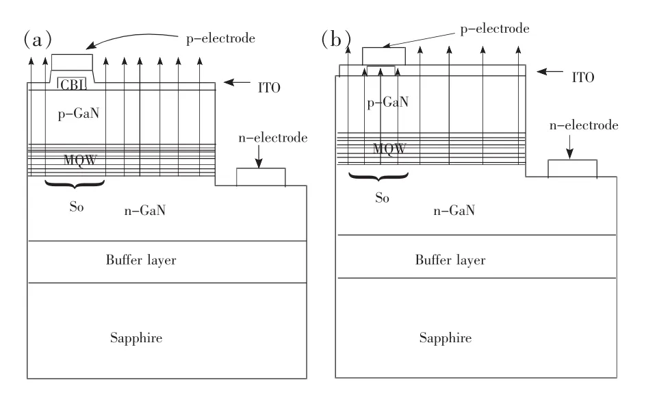
Fig.1 Schematic diagram of LEDs with(a)and without(b)CBL
Fig.2(a),(b),(c)are the images under the opticalmicroscope,and(a),(b),(c)shows the conventional structure of a LED(sample A),stripes roughened surface(sample B),the roughened LED with the side etching(Sample C),respectively.Three kinds of LED are fabricated at the same batch.All the process,such as ICP etching,lithography,cleaning,and alloy electrode growth were in the same conditions.Based on three different structures(sample A,B,C),another group of devices containing CBL were fabricated as sample D(A+CBL),E(B+CBL),F(xiàn)(C+CBL).At last,these samples were divided into three groups,each group contained two LEDs.All the data obtained were from PMS-80 SYNC-SKAN SPECTRO PHOTOCOLORIMETER test system.
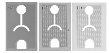
Fig.2 The top view of LED for three structures.(a)Conventional.(b)Surface roughing.(c)Surface roughing+SWE(side wall etching).
Fig.3 shows I-V curves of four kind of LEDs,and Fig.4 shows the output power of three groups of LEDs.From Fig.3 and Fig.4,we can de monstrate that the output power of the LEDswith CBL are larger than those without CBL,but the voltages are a little higher.It shows that these LEDs with CBL have a better current spreading effect,the effective current get improved,and the probability of the carrier radiation emitting get increased,too.Thus the luminous efficiency and device performance get improved.Themajority of current flow to the active region,which is not vertically below the electrode part,increases the current expansion,and it also reduces the consumption of current vertically below the electrode part effectively,so it causes less heat at the same part.The CBL prevents the injection current from flowing through the active region.ITO film growing on the current blocking layer can also be benefit for currentexpansion,and italso increase the transmission of the light with the corresponding wavelength.The combination of the ITO and CBL makes current spreadingmuch well.And the smaller the size of LED is,the better the current spreading is.We can get a vivid image from Fig.5.The LED with CBL getsmore effective area in the active region than those without CBL,and the current is also more uniform.

Fig.3 I-V characteristic of the 4 kinds of chips

Fig.4 Output power of three groups of LED.(a)Conventional structure and a CBL structure.(b)Surface roughing+CBL structure and surface roughing structure.(c)Surface roughing+CBL+SWE(side wall etching)structure and surface roughing+SWE structure.
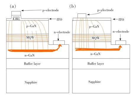
Fig.5 The current spreading in LED with(a)and without CBL(b).
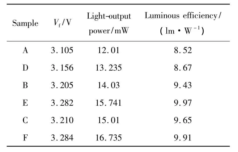
Table 1 Data of the samp les
Fig.6 shows the luminous efficiency of different structures.Table 1 lists the parammeterts six kinds of LEDs.All the data aremeasured at the inject current of 20 mA.Sample A is the conventional structure and D is the conventional structure with CBL,sample B is the structure with surface roughing and E is the structure with CBL,sample C is the structure with surface roughing+side wall etching and F is the structure with CBL.Table 1 shows that the forward voltags of the CBL structure are slightly higher than that without CBL,and the optical characteristics get improved.The light-output power of sample D,E,F(xiàn) are 10.19%,12.19%,11.49%higher than A,B,C.The luminous efficiency are 1.76%,5.72%,2.69%higher.
It is found that the voltages of surface roughening structure and surface roughing+side wall etching are slightly higher than the normal one,the surface roughing process will damage the ITO surface and impact the current spreading.
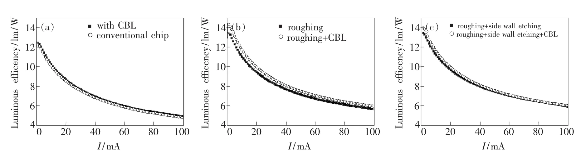
Fig.6 Luminous efficiency of deferent structures.(a)Conventional structure and a CBL structure.(b)Surface roughing+CBL structure and surface roughing structure.(c)Surface roughing+CBL+SWE(sidewall etching)structure and surface roughing+SWE structure.
4 Conclusion
In summary,six kinds of LEDswith the same size were fabricated successfully and the optoelectronics properties of the same batch products were researched.The experimental results show that the light-output power and the luminous efficiency can improved by depositing a current blocking layer,although the forward voltage is slightly higher.The process is very simple and cheap,and it can be widely used in modern LED production.The follow-up work should be concentrate on how to optimize the process condition and reduce the forward voltage.
[1]Yin H B,Wang X L,Ran JX,etal.High quality GaN based LED epitaxial layers grown in a homemade MOCVD system[J].J.Semicond.,2011,32(3):0330021-1-4.
[2]Jeong H H,Lee SY,Jeong Y K,etal.Improvementof the lightoutput power of GaN-based vertical lightemitting diodes by a current blocking layer[J].Electrochem.Solid-State Lett.,2010,13(7):H237-H239.
[3]Lin Y C,Chang S J,Su Y K,et al.High power nitride based light emitting diodes with Ni/ITO p-type contacts[J].Solid-State Electron.,2003,47(9):1565-1568.
[4]Zhou Z,F(xiàn)eng SW,Zhang G C,etal.The aging characteristics ofhigh-power GaN-based white light-emitting diodes[J].Chin.J.Lumin.(發(fā)光學(xué)報(bào)),2011,32(10):1046-1050(in Chinese).
[5]Wang W J,Li X F,Shi JF,et al.Effect of ITO interfacemodulation layer on the performances of LEDs with Ga-doped ZnO electrode[J].Chin.J.Lumin.(發(fā)光學(xué)報(bào)),2012,33(2):210-215(in Chinese).
[6]Xu XW,Cui B F,Zhu Y X,et al.Research of dielectric photonic crystal on red LED to increase luminous flux[J].Acta Phys.Sinica(物理學(xué)報(bào)),2012,61(15):154213-1-5(in Chinese).
[7]Linder N,Kugler S,Stauss P,et al.High-brightness AlGaInP light-emitting diodes using surface texturing[J].SPIE,2001,4278:19-25.
[8]Pan H P,Huang LW,Li R,et al.Finite elementmodel of GaN based LED and the optimization of themesa structure[J].Chin.J.Lumin.(發(fā)光學(xué)報(bào)),2007,28(1):114-120(in Chinese).
[9]Zhang Y H,Guo W L,GaoW,etal.Properties of the ITO layer in a novel red light-emitting diode[J].J.Semicond.,2010,31(4):0430021-1-5.
[10]Wang H C,Su Y K,Lin C L,etal.InGaN/GaN light emitting diodeswith a lateral currentblocking structure[J].Jpn.J.Appl.Phys.,2004,43(4B):2006-2007.
[11]Huh C,Lee J,Kim D,et al.Improvement in light-output efficiency of InGaN/GaN multiple-quantum well light-emitting diodes by current blocking layer[J].J.Appl.Phys.,2002,92(5):2248-2250.
[12]Guo E Q,Liu Z,Qiang W,et al.Optical and electrical characteristics of GaN vertical light emitting diode with current block layer[J].J.Semiconductors,2011,32(6):0640071-1-4.
[13]Deng Y L,Liao C J,Liu SH,et al.Calculating external quantum efficiency of high bright light emitting diodes[J].Chin.J.Quant.Electron.(量子電子學(xué)報(bào)),2002,19(1):65-69(in Chinese).
