Field Em ission Characteristics of Single W all Carbon Nanotube Rope at The Presence of Dielectric M edium
2013-03-02 07:13:52GAOJianTONGYuXIAFengLIUJunxiuZENGYou
發光學報 2013年7期
GAO Jian,TONG Yu* ,XIA Feng,LIU Jun-xiu,ZENG You
(1.School of Materials Science and Engineering,Shenyang Jianzhu University,Shenyang 110168,China;2.Shenyang National Laboratory for Materials Science,Institute of Metal Research,Chinese Academy of Sciences,Shenyang 110016,China)
*Corresponding Author,E-mail:tong_yu123@hotmail.com
1 Introduction
Carbon nanotube(CNT)is generally considered as one of the best field emitters due to its superb structure and properties including nanoscale radius of curvature,high aspect ratio,excellent electrical conductivity,outstandingmechanical stiffness and chemical inertness.Some electron sources based on CNT field emitters have been developed for the potential applications in field emission display(FED)[1-3],back light source for liquid crystal display(LCD)[4-5],cathode-ray lighting element[6-7],gasdischarge tube[8],electron gun for scanning electron microscopy(SEM)[9]or X-ray generator[10-11].
In these vacuum electron devices,a third electrode,generally named the focusing gate,is used to control the electron trajectories from CNT field emitters[3,12-13],which inevitably increases the complexity and cost.In order to simplify the structure for electron trajectory controlling,some self-focusing electron sources have been proposed by positioning the gate electrode parallel with the emitter vicinity[14]or at the center of cathode[15].In previous work,a relative simple way was proposed to control the electron trajectories by selecting presence of dielectric medium such as glass flakes near the single-wall carbon nanotube(SWCNT)rope as field emitter[16],but the contribution of geometric dimension of the dielectric medium was not investigated and discussed in details up to now.In thiswork,theoretic analysis and evidentialmeasurements were carried out to reveal themodification of electric field at the presence of dielectric medium in diode structure and its influence on the field emission characteristics of the SWCNT rope.A feasible way is proposed for fabricating electron sources with controllable electron trajectories.
2 Experiments
2.1 Preparation of SWCNT Rope Field Em itter
Macroscopically long ropes of aligned SWCNTs synthesized by amethod of arc discharge[17]were obtained from Advanced Carbon Division,Institute of Metal Research,Chinese Academy of Sciences.Under SEM observations,the SWCNT rope as demonstrated to bemade up of tightly packed,roughly aligned bundles of SWCNTs,and few bundles were found to stretch out from the sidewall of the SWCNT rope(Fig.1(a)).A simple cut by a razor blade was performed to obtain a great number of SWCNT tips at the emitting surface of SWCNT rope for field emission,as shown in Fig.1(b).
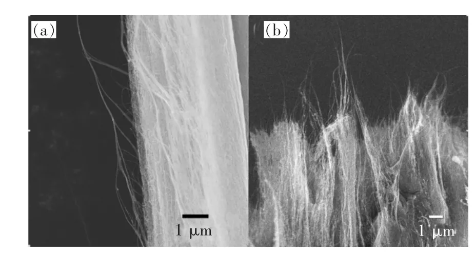
Fig.1 Typical SEM images of SWCNT ropes.(a)The sidewall.(b)The emitting surface.
2.2 Field Emission Measurements of SWCNT Rope
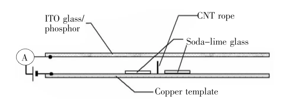
Fig.2 Diode structure used for the field emission measurements of a freestanding SWCNT rope surrounded by glass flakes
Fig.2 shows the diode structure we used to determine the field emission performance from a freestanding rope of SWCNT,in which the SWCNT rope was fixed perpendicularly onto a copper plate cathode.An indium-tin-oxide(ITO)glass was employed as the anode to collect emission electrons,and the gap between the SWCNT tips and the anode was about 1mm.Two flakes of soda-lime glass(12 mm×9 mm×1 mm in dimension)were symmetrically positioned on each side of the SWCNT rope,and the separation distance and thickness of the glass flakes could be adjusted arbitrarily.The diode structure was transferred into a high vacuum chamber,in which the working pressure was typically of the order of 10-5Pa.Keithley PS350 High Voltage Supply and 2000 Multimeter were used to provide the bias voltage with a step of 3 V and to record the emission current,respectively.
3 Results and Discussion
Fig.3 shows the shifts of field emission characteristics from the same SWCNT rope with and without the presence of glass flakes.From Fig.3,an abrupt jump of the emission current(2.5~141.5 A)at a threshold voltage of~670 V can be easily distinguished from the I-V curve at the presence of glass flakes(see the opened squares in Fig.3),which gave rise of a relative high current after the current jump.Meanwhile,a selective expansion of the electron patternswas found with the current jump,indicating the divergence of electron trajectories due to the modification of electric field at the presence of glass flakes.
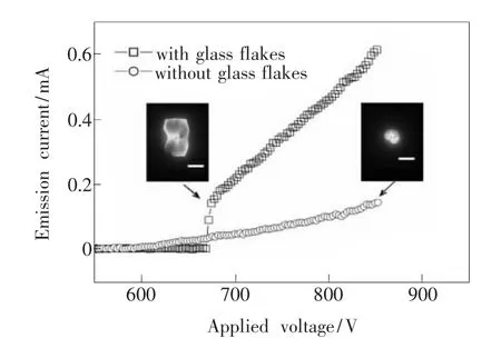
Fig.3 Comparisons of the I-V alternations from the same SWCNT rope with(opened square)and without(opened circle)glass flakes,along with the corresponding electron patterns atan equivalent currentof~145 A.The length of the SWCNT rope was 3.15 mm,and a scale bar of 12 mm was involved into the optical insets.
With the application of Gauss theorem in electrostatic field,once a sheet of dielectric substance is introduced into the plate electrodes under a constant potential of U,the electric field strength(E)between the dielectric sheet and the electrode can be roughly estimated by the following equation,
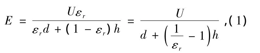
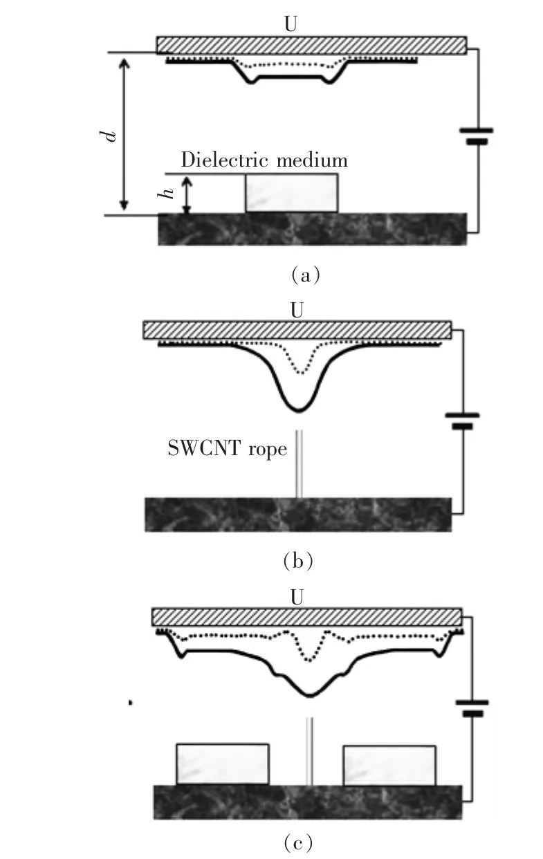
Fig.4 Schematic diagrams of the electric field distribution in a diode structure at the presence of dielectric medium only(a),isolated SWCNT rope(b),and a SWCNT rope positioned between two dielectric flakes(c).
in which,U and d is the potential and distance between two electrodes,respectively,while h and εris the thickness and relative dielectric constantof the dielectric medium.Since the value ofεris higher than 1,i.eit is obviously that the E value obtained from Equation(1)is higher than that without the presence of dielectric mediumTherefore,an assumed distribution of the electric field at the presence of dielectricmedium can be illustrated as Fig.4(a),in which the edge effect of induced charge distribution has been also taken into account.On the other hand,a SWCNT rope field emitter placed between the plate electrodes would generate an electric field roughly following the simple quadratic distribution[3](Fig.4(b)),and consequently,by making use of the superposition principle,the distribution of electric field near a SWCNT rope at the presence of glass flakeswas obtained and shown in Fig.4(c).The modification of electric field shown in Fig.4(b)~(c)can be used to explain the peculiar phenomena mentioned above.While the simple quadratic distribution of electric field around the isolated SWCNT rope(Fig.4(b))aroused a circle-like electron pattern,the separated peaks of electric field distribution in Fig.4(c)would result in the divergence of electron trajectories at high fields and thus give rise of the expanded patterns of electron patterns at the presence of dielectric medium.Since the spreading of emitting electrons over a relatively large region is helpful to reduce the adverse influence of space charge effect on electron emission[18],the corresponding emission current would increase to some extent,as shown in Fig.3.In the meanwhile,it should be pointed out that the small trough of electric field distribution near the SWCNT rope at low fields(see the dotted line in Fig.4(c))could be taken as an activation barrier for electrons to emit from the SWCNT tip.Only when the applied voltage is high enough to overwhelm this activation barrier,part of the emitted electrons would fly towards the glass edge and then generate the expanded emission patterns shown in Fig.3.
It is suggested by equation(1)that the electric field E must be strongly dependent upon the parameters of h andεr.In an evidential investigation,while the thickness of glass flakes(h)near a SWCNT rope(3.15 mm in length)was increased step by step,the amplitude and threshold voltage for the current jump were found to increase apparently until the glass flakes were higher than the SWCNT rope,as shown in Fig.5(a).According to equation(1),any increase of the glass thickness(h)would result in an increment of the electric field E,and thus generated a deeper barrier and a higher threshold voltage for the occurrence of current jump.On the other hand,since the region for electron pattern expansion kept unchanged with increasing glass thickness,the space charge density around the SWCNT tip did not change apparently,and thus result in the similar I-V alternations after the current jump(Fig.5(a)).Once the glass thickness(h=4.0 mm)was larger than the height of SWCNT rope(3.15 mm),the existence of so thick glass flakes would partly block the paths of electron emission,and consequently result in a less amplitude and relative low threshold voltage for the current jump.
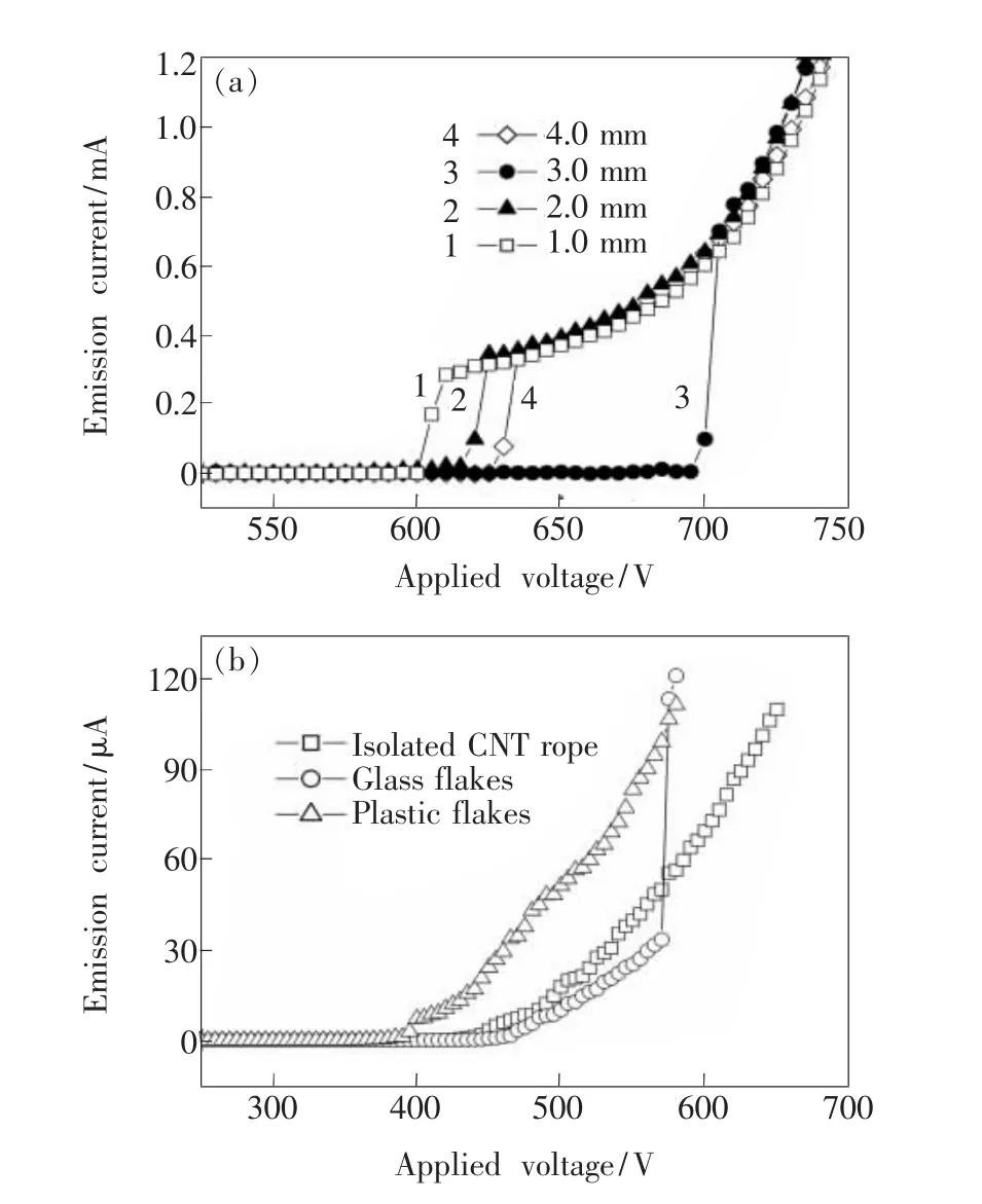
Fig.5 Shifts of the I-V alternations from the same SWCNT rope in terms of the glass thickness(a),and the presence of dielectric mediums based on PE plastic or Soda-lime glass(b),respectively.
Moreover,equation(1)suggested that a relatively low dielectric coefficientεrwould give rise of a decreased electric field of E,and thusmake a less contribution to the corresponding I-V alternations.Accordingly,several dielectric medium,whose value of dielectric constanthas been determined by using a bridgemeasurement,was employed to take the place of glass flakes.In Fig.5(b),the glass flakes(εr=5.45)was substituted by polyethylene flakes(εr=2.26)in similar size for the I-V measurements,in which only a slight jump of the emission current could be observed at the presence of plastic flakes.In other investigations,quartz glass(εr=3.72),alumina(εr=6.86),or ceramic mat(εr=6.11)behaved similar current jump to that of soda-lime glass,while the presence of softmaterials with low dielectric constant,such as plastic or rubber flakes in similar size did not arouse notable jump of the emission current.
Additionally,it should be pointed out that only while the dielectric medium is close enough to the field emitter,the shifts ofI-Valternations can be detected obviously.Fig.6 shows the influence of the enlarged separation distance between two glass flakes on theI-Valternations from the same SWCNT rope,in which a gradually decreased amplitude for the current jump,along with a higher threshold voltage and amuch less enhanced emission current athigher field,can be observed.
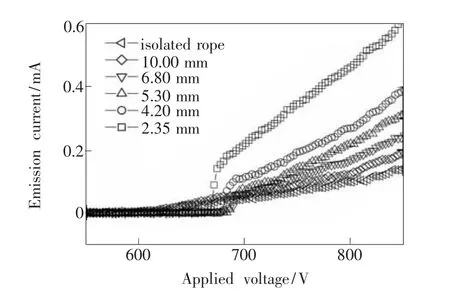
Fig.6 Shifts of the I-V alternations in terms of the separation distance between glass flakes
The phenomena described above indicate an interesting and feasible way to control the field emission characteristics including emission current and electron patterns from Spindt-type field em itters including SWCNT ropes by adjusting the dielectric constant or configurations of surrounding substance.It is very promising for the fabrications of electron sources used in back light source for LCD,cathode lighting elements and X-ray generators.
4 Conclusion
In the diode structure for field emission measurements of SWCNT rope,the introduction of dielectric medium such as glass flakes aroused an intriguing jump of the emission current,along with a selective expansion of the electron patterns and an enhanced current after the jump.The phenomenawere attributed to themodification of electric field at the presence of dielectrics,which is strongly depending on the dielectric constant and configurations of dielectric medium.This result gives a possibility of designing a new vacuum device with high emission current and controllable electron patterns.
Acknow ledgements:The authors present great thanks to Prof.Huiming Cheng,Prof.Chang Liu in Institute of Metal Research,Chinese Academy of Sciences and Prof.Younghee Lee,Dr.S.C.Lim in Department of Physics,Sungkyunkwan University,R.Korea for their helpful advices and discussion related to thiswork.
[1]Kim JM,ChoiW B,Lee N S,et al.Field emission from carbon nanotubes for displays[J].Diam.Relat.Mater.,2000,9:1184-1189.
[2]Wu C,Li TH,Guo TY.Fabrication and optimization of carbon nanotube field emitters for flat-panel display device[J].Mater.Sci.Forum.,2011,663-665:800-803.
[3]Lan Y C,Lee C T,Hu Y,et al.Simulation study of carbon nanotube field emission display with under-gate and planargate structures[J].J.Vacuum Sci.Technol.B,2004,22(3):1244-1249.
[4]Kim Y C,Kang H S,Cho E,et al.Building a backlight unitwith lateral gate structure based on carbon nanotube field emitters[J].Nanotechnol.,2009,20(9):095204-1-7.
[5]Liu ZC ,Li Y A,Wang J,etal.Field emission characteristics of carbon nanometer ball films[J].Chin.J.Liq.Cryst.Disp.(液晶與顯示),2012,27(3):297-302(in Chinese).
[6]Saito Y,Uemura S.Field emission from carbon nanotubes and its application to electric devices[J].Carbon,2000,38(2):169-182.
[7]Jang Y T,Lee Y H,Ju B K,et al.Application of carbon naotubes to the cathode ray tube-electron gun[J].Vacuum,2002,68(1):79-85.
[8]Rosen R,Simendinger W,Debbault C,et al.Application of carbon nanotubes as electrodes in gas discharge tube[J].Appl.Phys.Lett.,2000,76(13):1668-1670.
[9]Nakahara H,Ichikawa S,Ochiai T,etal.Carbon nanotube electron source for field emission scanning electronmicroscopy[J].J.Surf.Sci.Nanotechnol.,2011,9:400-403.
[10]Wang SG,Calderon X,Peng R,etal.A carbon nanotube field emissionmultipixel X-ray array source formicroradiotherapy application [J].Appl.Phys.Lett.,2011,98(21):213701-1-3.
[11]Zhang Y P,Lau S,Huang L,et al.Carbon nanotubes synthesized by biased thermal chemical vapor depositions as an electron source in an X-ray tube[J].Appl.Phys.Lett.,2005,86(12):123115-1-3.
[12]Zhong SX,LiGS,Li ZH,etal.Experiment research on carbon nanotube field emission performancewith flatgrid structure[J].Chin.J.Lumin.(發光學報),2009,30(1):119-122(in Chinese).
[13]Zang F H,Ding G F,Wang Y,et al.Characteristics of the three-dimensional trapezoidal electrodes for carbon nanotube field emitters[J].Vacuum,2010,85(1):48-54.
[14]Lin K C,Chen HW,Juan C P,et al.Carbon-nanotube-based field emission devices with a self-focusing gate structure[J].J.Electrochem.Soc.,2008,155(3):K38-K41.
[15]Yuan G,Jiang JJ,LiC,etal.Simulation of self-focusing electron emitter[J].J.Vac.Sci.Technol.B,2010,28(3):627-630.
[16]Tong Y,Lim SC,Park K G,et al.Controlling field-emission patterns of isolated single-wall carbon nanotube ropes[J].Appl.Phys.Lett.,2005,87(4):043114-1-3.
[17]Liu C,Cheng H M,Cong H T,etal.Synthesis ofmacroscopically long ropes ofwell-aligned single-wall carbon nanotubes[J].Adv.Mater.,2000,12(16):1190-1192.
[18]Zhang Q,Chen Z X,Zhu B J,et al.Space charge effect in carbon nanotube field emission[J].Chin.J.Lumin.(發光學報),2008,29(3):567-572(in Chinese).
