Electronic structures and optical properties of substitutional and interstitial N-doped ZnO
2020-05-14 04:21:00DONGMingHuiLIXiaoJieTANGShunLei
原子與分子物理學報 2020年2期
DONG Ming-Hui,LI Xiao-Jie,TANG Shun-Lei
( Qilu Institute of Technology,Jinan 250200,China)
Abstract:In this paper,the formation energies,electronic structures and optical properties of substitutional and interstitial N-doped ZnO were calculated by density functional theory (DFT).The results show that the N atom prefers to octahedral interstitial site because of low formation energy.The p-type ZnO is obtained by N doping,and N atom at interstitial site can narrow band gap width obviously,which will improve the solar light absorption and utilization.In the energy region of visible light,the N atom at interstitial site has a good absorption spectrum of visible light and results in redshift significantly,which is consistent with the band gap width change regulation.
Key words:Optical properties;Electronic structure;ZnO;First-principles
1 Introduction
Wurtzite ZnO is a kind of wide-band-gap II-VI semiconductor,which band-gap is 3.37 eV[1],and binding energy is 60 meV[1]at room temperature.ZnO does not only exhibit excellent physical and chemical properties but is also characterized by rich raw materials,low cost,and environmental friendliness.Due to its excellent physical and chemical,ZnO has many technological applications,such as photocatalysis,transparent conductive films,blue/ultraviolet (UV) light-emitting diodes and lasers,UV detectors,and so on[2-8].As we know,the preparation of high quality p-type ZnO thin films is critical for its practical application.In order to fabricate good p-type material,doping is an effective method[9,10].In p-type doping group-V elements,N relative to P and As,is supposed to be ideal candidate for p-type dopant in ZnO[11-13].
In order to grow stable p-type ZnO,various strategies have been employed in the literature to enhance the nitrogen solubility in ZnO[14-16].Among different reported techniques,element co-doping and modification is regarded as the most effective way to improve the photocatalytic performance via influencing the crystal internal structure or moving the Fermi level[17].Therefore,many groups have carried out theoretical and experimental studies to realize p-type ZnO by the co-doping method using different dopants such as Co-N[18],S-N[19],Be-N[20],Ag-N[21],Li-N[22],Al-N[23,24],etal.It should be pointed out that all the experimental and computational results of N doped ZnO in these literatures are not in consideration of the site effect of N on ZnO,and there is a lack of studies regarding interstitial N atoms.In fact,it is quite possible for N to occupy the interstitial positions of the ZnO lattice due to its small atomic radius (about 0.75 ?).Guanetal[25]and Kongetal[26,27]have already investigated the effect of substitutional and interstitial P,Be,H atoms on electronic structure and optical properties of ZnO using first-principle calculation,respectively.Therefore,in this paper,the band structures,total and partial density of states (TDOS and PDOS) and optical properties of N as substitutional and interstitial atom in ZnO are investigated using first-principle calculation.The results will provide new perspective for understanding the mechanism of N doped ZnO and developing high effective photocatalytic materials based on ZnO.
2 Computational process
2.1 Computational methods
All of the calculations were performed using first-principle based on DFT[28,29].Generalized gradient approximation (GGA) and the Perdew-Burke-Ernzerhof (PBE)[30]function were employed as exchange-correlation potential.The interaction between valence electron and ion core was ultrasoft pseudopotential.The valence electron configurations for Zn,Al,O,N were considered as 3d104s2,3s23p1,2s22p4and 2s22p3,respectively.The cut off kinetic energy was set as 380 eV and Monkhorst-Pack[31]k-points were chosen to 4×4×2 in the Brillouin zone to ensure that all of the calculations were converged.For the geometry optimization process,the energy change and the maximum tolerances of the force,stress,and displacement were set to 2.0×10⁻⁵eV/atom,0.05 eV/?,0.05 GPa and 0.002 ?,respectively.It is well known that the DFT underestimates the width of the fundamental gap by about 30% for the excited state of multiparticle system.Therefore,we used an orbital-dependent potential that added an extra Coulomb interactionU(GGA+U)[32].In this paper,Ud,Zn= 10.0 eV for Zn 3dandUp,O= 7.0 eV for O 2pwere adopted in the GGA +Umethod[33].
2.2 Theoretical models
To build the N-doped systems,one N atom is added,respectively,at four positions of the ZnO lattice,i.e.,the two substitutional positions (s1and s2),where the Zn and O atoms are replaced by the N atom,respectively,and the two interstitial positions of tetrahedral interstitial site (i1) and octahedral interstitial site (i2).Fig.1 shows the schematic illustrations of the crystal structures of ZnO with the N atom at the four doping positions of s1(Fig.1b),s2(Fig.1c),i1(Fig.1d) and i2(Fig.1e),respectively.
3 Results and discussion
3.1 Geometry optimization results
The lattice parameters of pure ZnO were obtained by geometry optimization,as shown in Table 1.
It is found that the calculated results (a=b=3.267 ?,c=5.276 ?) are in good agreement with theoretical[17,33-35]and experimental results (Vispute[36]:a=b=3.249 ?,c=5.206 ?;Decremps[37]:a=b=3.258 ?,c=5.220 ?),with a deviation less than 2%.The comparison of theoretical and experimental results suggests that the present GGA+Umethod is relatively reasonable.

Fig.1 Schematic illustrations of the crystal structures of (a) pure ZnO and the N atom at the positions of (b) s1,(c) s2,(d) i1 and (e) i2.
Table 1 Comparison of several properties of ZnO of the present work,theoretical and experimental results in the literature.The listed are lattice constanta,b,candc/aratio
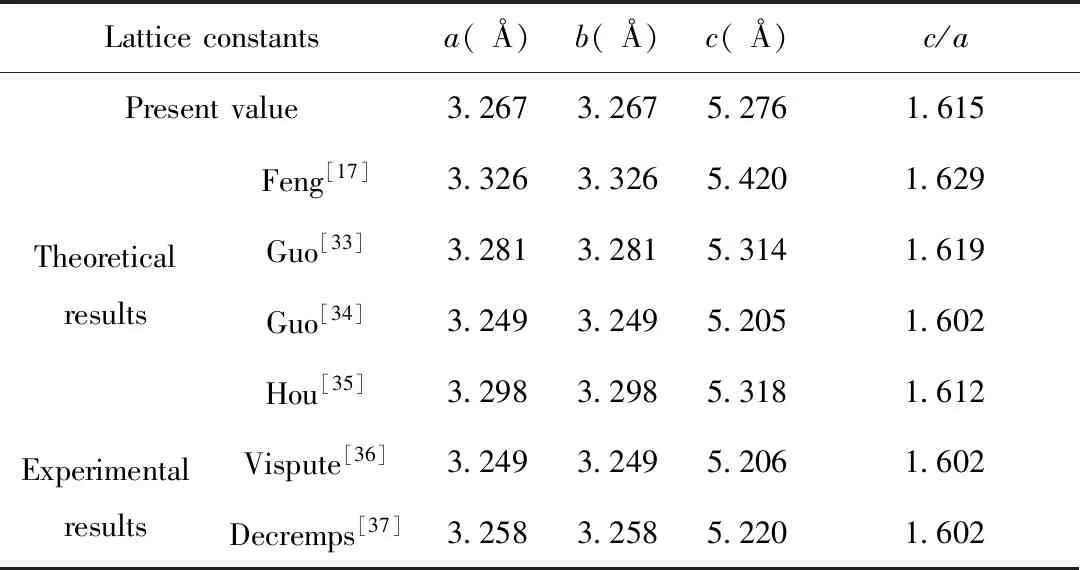
Latticeconstantsa(?)b(?)c(?)c/aPresentvalue3.2673.2675.2761.615TheoreticalresultsFeng[17]3.3263.3265.4201.629Guo[33]3.2813.2815.3141.619Guo[34]3.2493.2495.2051.602Hou[35]3.2983.2985.3181.612ExperimentalresultsVispute[36]3.2493.2495.2061.602Decremps[37]3.2583.2585.2201.602
3.2 Impurity formation energy
In order to understand relative stability of a doping system and the degree of difficulty of atomic doping,it is necessary to calculate the formation energy(Ef).If the calculatedEfis smaller,meaning that the structure is more stable and more favorable in experiment.In this paper,we calculate the formation energy by the following formulas defined by Walle[38,39].
Ef(ZnO)=E(ZnO)-μ(Zn)-μ(O)
(1)
Ef(s1)=E(s1)-E(ZnO)+μ(Zn)-μ(N)
(2)
Ef(s2)=E(s2)-E(ZnO)+μ(O)-μ(N)
(3)
Ef(i1)=E(i1)-E(ZnO)-μ(N)
(4)
Ef(i2)=E(i2)-E(ZnO)-μ(N)
(5)
whereEf(ZnO),Ef(s1),Ef(s2),Ef(i1),Ef(i2) are formation energies of pure ZnO and the N atom at the positions of s1,s2,i1and i2,respectively.E(ZnO),E(s1),E(s2),E(i1),E(i2) are their total energy,respectively.Theμ(Zn),μ(O) andμ(N) stand for the chemical potentials of Zn,O and N,respectively.During simple preparation,μ(O)=E(O2)/2,E(O2) is the oxygen molecule total energy,μ(N)=E(N2)/2,E(N2) is the nitrogen molecule total energy andμ(Zn)=E(Zn)bulk,E(Zn)bulkis very close to each Zn atom energy in bulk Zn.The calculated chemical potentials in our work are:μ(Zn)=-4.923 eV,μ(O)=-4.845 eV,μ(N)=-7.954 eV.The formation energies of various doped systems are given in Fig.2,and it can be found that formation energy of pure ZnO is -3.65 eV,which is compared to the experimental value of -3.6 eV[40]and the previous theoretical result of -3.59 eV[41].Formation energies for four N doped ZnO positions are all negative,which imply that all structures are energetically stable.In addition,one could also observe from Fig.2 that thei2has the lowestEfvalue (-6.21 eV) among the four doping positions,implying that the N atom at octahedral interstitial site is the most stable structure and the most likely to be formed in experiments.Compared pure ZnO and s2,it can be found that the difference ofEfvalue between pure ZnO (-3.65 eV) and s2(-3.93)is very little.This is because the radius and electronic structure of N and O atoms are very similar.Therefore,the lattice distortion caused by substitution of N atom for O atom is very small.
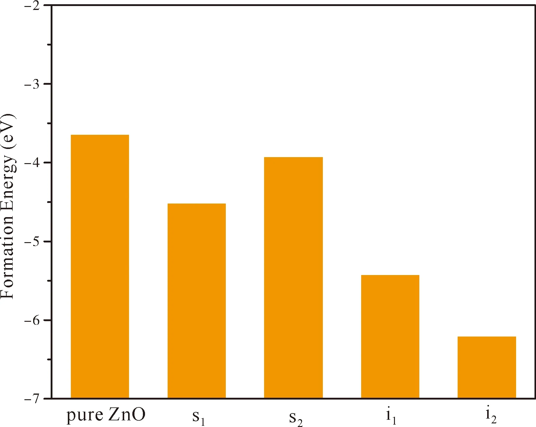
Fig.2 The formation energies of pure ZnO andthe N atom at the positions of s1,s2,i1 and i2.
3.3 Electronic structures
3.3.1Bandstructure
As shown from Fig.3(a),the conduction band minimum (CBM) and valence band maximum (VBM) are all located in the G-point of Brillouin zone,which indicates that ZnO is a direct band-gap semiconductor.The calculated band gap of pure ZnO withUd,Zn= 10.0 eV for Zn 3dandUp,O= 7.0 eV for O 2p(Uis Hubbard coefficient) in this paper is 3.35 eV,which is in agreement with the experimental value[1].Therefore,these values ofUare used in the following work for the electronic structures and optical properties of N doped ZnO.
Fig.3(b)~Fig.3(e) show the calculated band structures of s1,s2,i1and i2,respectively,and the corresponding band gaps are 3.02 eV,3.13 eV,2.89 eV and 2.68 eV,respectively.All of the band gaps of four doping systems are narrower than that of pure ZnO.In the meanwhile,the VBM of ZnO after N doping shifts up into the upper part of the Fermi level in the band gap,eg.,the VBM of s1,s2,i1and i2are located at 0.19 eV,0.11 eV,0.51 eV and 0.73 eV,respectively.From above discussions,we know that the p-type ZnO is obtained by N doping.The p-type doping characteristics make the doped states appear in the upper part of the Fermi level in the band gap of the doped ZnO,leading to the expansion of the valence band to the higher energy region.These impurity states near the Fermi level serve as springboard under excitation,which are benefit for the transfer of the photogenerated electrons to the CB,improving the solar light absorption and utilization,and thus enhance the photocatalytic properties of doped ZnO[42].
3.3.2Densitiesofstates(DOSs)

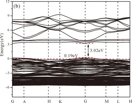
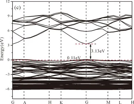
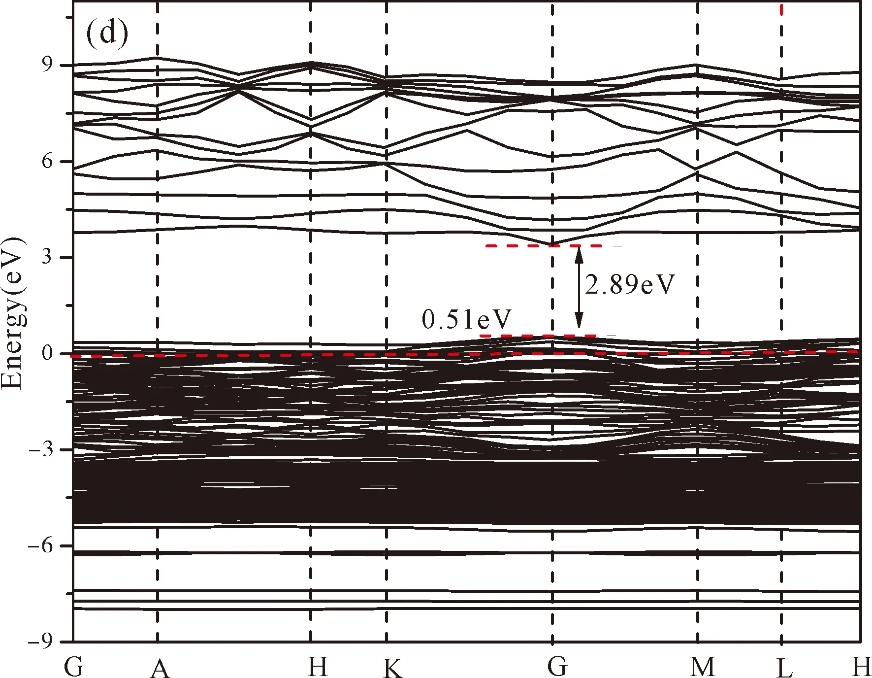
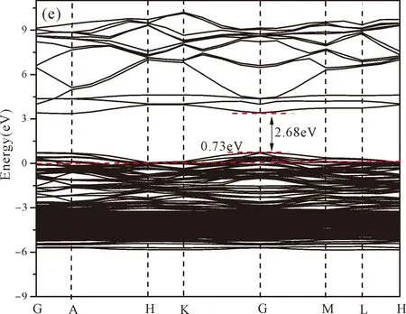
Fig.3 Band structures of (a) ZnO,and ZnO with doping of N at (b) s1,(c) s2,(d) i1,and (e) i2
Fig.4(a)~Fig.4(e) show the DOSs in pure ZnO and different doping cases,including the total DOSs (TDOSs) and partial DOSs (PDOSs) of each atom.The dotted lines at the zero point of horizontal coordinates represent the Fermi level(EF) of pure ZnO and the doped ZnO.The valence band of pure ZnO is mainly composed of O-2p and Zn-3d states,and the conduction band mainly derives fromthe Zn-3p and the Zn-4s states as shown in Fig.4(a).It is believed that the change of the Fermi level of a semiconductor will definitely affect its photocatalytic properties.Therefore,it is necessary to research the changes of DOSs near the Fermi level caused by different doping sites.The details of DOSs for the doped ZnO are in Fig.4(b)~Fig.4(e).As shown in Fig.4,the band gap of ZnO after N doping is narrower than that of the undoped ZnO system due to the VBM shifting up into the upper part of the Fermi level,and the effect of N atom at the positions of tetrahedral interstitial site (i1) and octahedral interstitial site (i2) is more significant.This is consistent with the band gap width change regulation.Besides,the deficiency of outer electrons derived from the N results in the formation of the doping levels under CBM,and makes the conduction band move towards the lower energy direction,which can also shorten the width band gap.The calculation results of the DOSs manifest that doping the N atom could achieve p-type doping,which makes the DOS at the Fermi level increase and produces more vacancy levels above the Fermi level.These vacancy levels are composed of O-2p states and the N-2p,and thus the electrons at Fermi level can be excited easily and jump into higher energy region through vacancy levels.
3.4 Optical properties
As we all know,the interaction of a photon with the electrons in the semiconductor system can lead to the transitions between occupied and unoccupied states.In the linear response range,the optical material properties can be determined from the dielectric function[43,44]
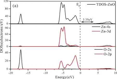
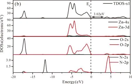
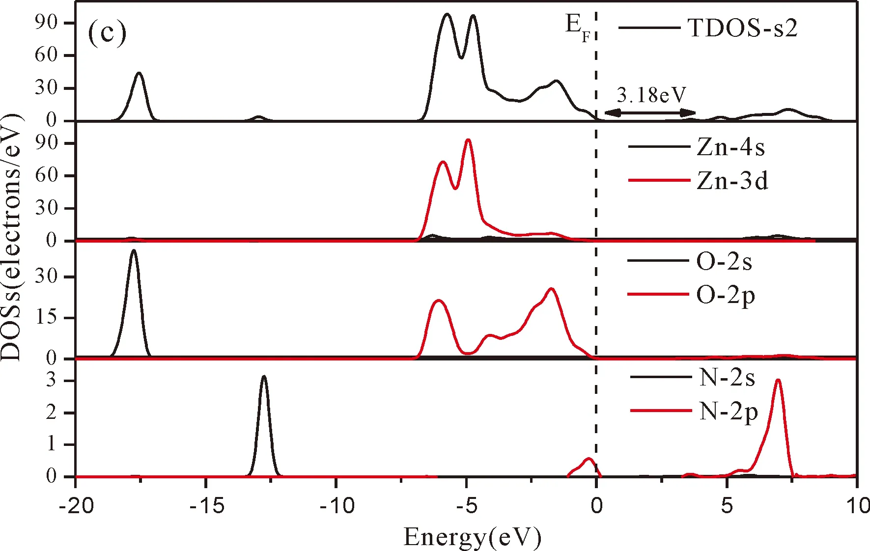
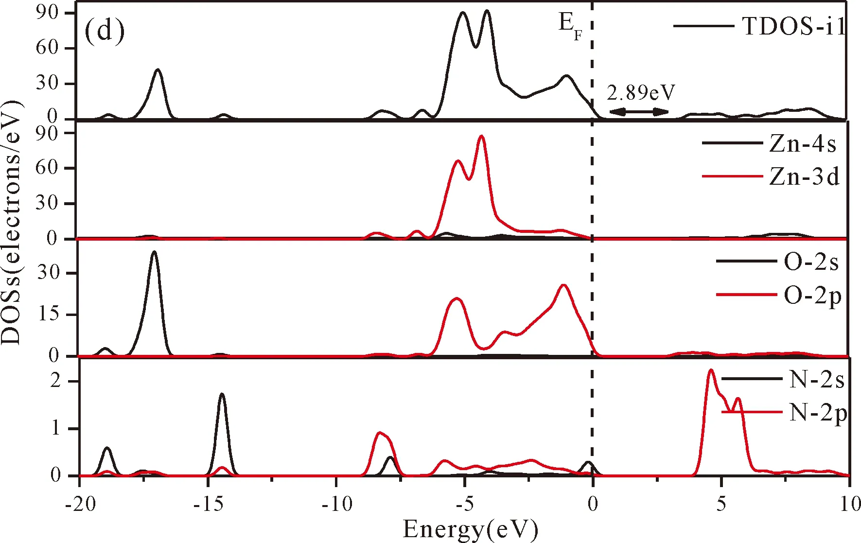
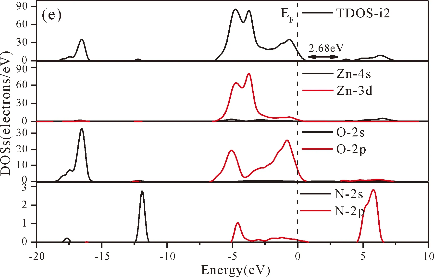
Fig.4 Density of states (DOSs) of (a) ZnO,and ZnO with doping of N at (b) s1,(c) s2,(d) i1,and (e) i2.
ε(ω)=ε1(ω)+iε2(ω)
(1)
(2)
|e·MCV(k)|2δ[EC(k)-EV(k)-?ω]
(3)
(4)
(5)
In theses equations,VandCrepresent valence bands and conduction bands,respectively.BZrepresents the first Brillouin zone,ωis angular frequency,kis the inverted sagittal,andEv(k) ,Ec(k) are the energy levels which located at valence band and conduction band,respectively.From the above functions(1)-(5),the optical properties,such as the absorption coefficient,reflectivity index are derived from the dielectric function.Equations (2) and (3) are also called Kramer-Kronig transformation.The above formulas provide a theoretical foundation for analysis of optical properties of the crystals,which reflects the emitting mechanism of the spectrum generated by the electronic transition between energy levels.
Fig.5 shows real part and imaginary part of dielectric function of pure ZnO and four doping systems.The imaginary part of dielectric function determines the probability that electrons absorb the energy of the incident photons and then electrons jump from the valence band to the conduction band.The bigger the imaginary part is,the more obvious the effect is[45].It can be seen that in the energy region (1.64-3.19 eV) of visible light,the imaginary part of the dielectric function of N doped ZnO is larger than that of pure ZnO,and i1and i2show much higher peaks.This is due to the valence bands of N doped ZnO moving up and the band gap decreasing.In the meanwhile,we can also see that the peaks of imaginary part (especially of N at tetrahedral interstitial site (i1) and octahedral interstitial site (i2)) shift to the low energy directions (red shift) relative to undoped ZnO.This is consistent with the band gap width change regulation.In addition,compared with pure ZnO,the imaginary partsε2(ω) of four doping systems have sharply increased in the low energy range from 0 to 5.0 eV and the increments of i1and i2are larger than that of s1and s2.Generally,N atom at interstitial site increases the corresponding values in the visible light region,enlarging the range of photoresponse.
Fig.5 real part is theε1(ω) of dielectric function.The calculated static dielectric constantsε1(0) for pure ZnO,s1,s2,i1,i2are 2.5,3.5,3.21,4.22 and 5.31,respectively.It can be seen from the real part of Fig.5 that the values ofε1(0) increase after N doping.However,it reveals that the obtainedε1(0) has inverse relation to the calculated band gap width (Eg),which agrees well with the relationship[46]of equation (6).
(6)
According to Lambert-Beer’s law[47],the absorption coefficientI(ω) is proportional to the absorbanceA(ω).The absorption coefficientsI(ω) of pure and four doping systems are plotted in Fig.6.In the energy region (1.64-3.19 eV) of visible light,I(ω) of four doping systems increases obviously,(especially of N at tetrahedral interstitial site (i1) and octahedral interstitial site (i2)),reaching 50000-70000 cm-1in the energy region of 2-4 eV.However,in the energy region of visible light,theI(ω) of pure ZnO is less than 20000 cm-1.Therefore,N at tetrahedral interstitial site (i1) and octahedral interstitial site (i2) is useful for absorption of visible light.
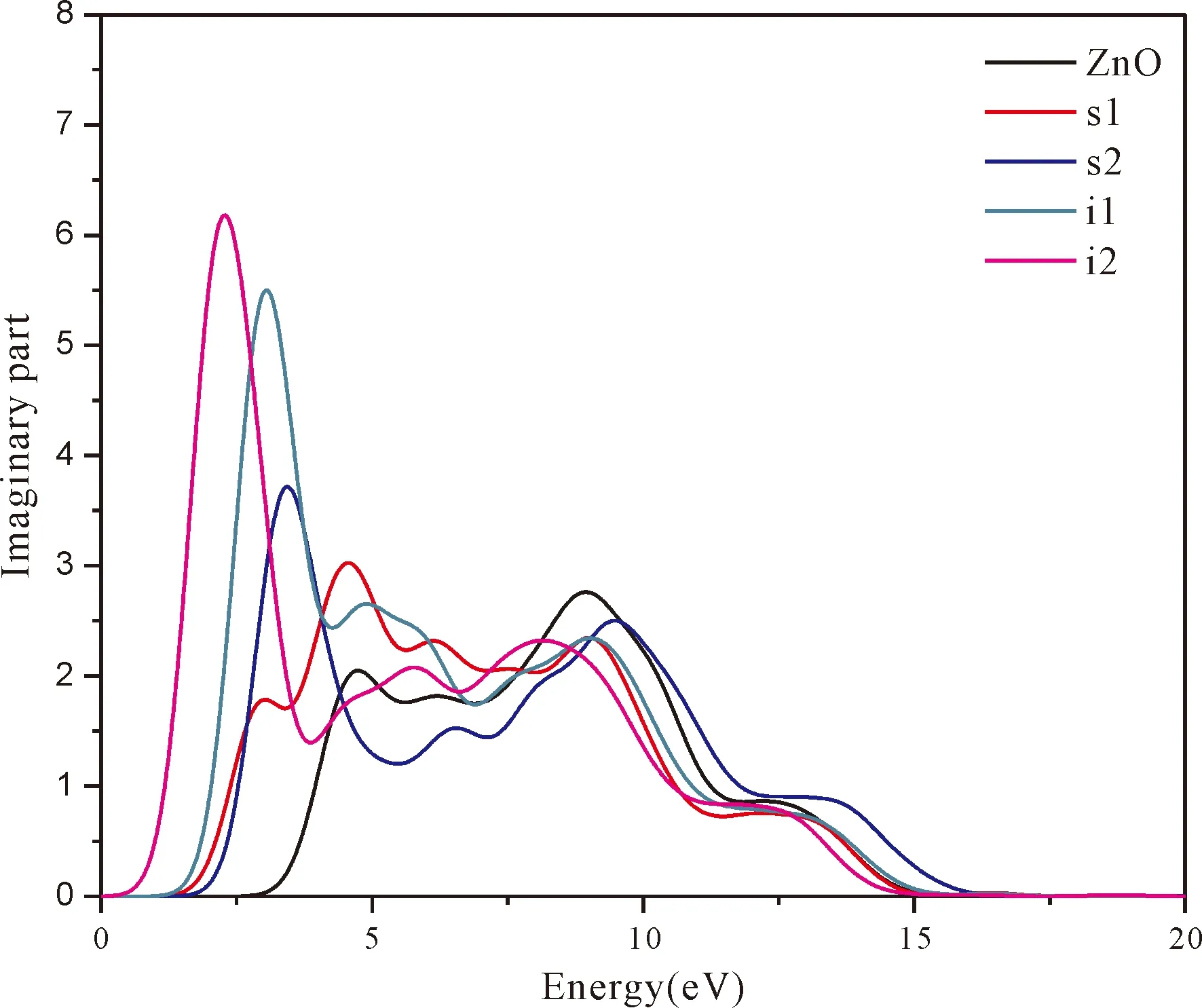

Fig.5 The dielectric function of pure andfour doping systems
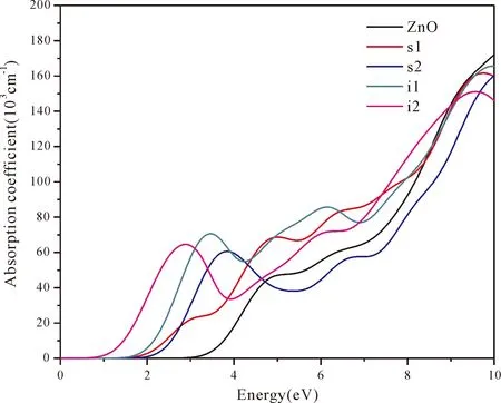
Fig.6 The absorption coefficient spectra of pure and four doping ZnO
4 Conclusions
In this study,we systematically analyze geometrical parameters,electronic structures and optical properties for substitutional and interstitial N-doped ZnO by using first principle calculation.The obtained conclusions are as following.
(1) The analyses of defect formation energy show that the N atom prefers to octahedral interstitial site.
(2)Band structure and DOSs show that the p-type ZnO is obtained by N doping.N atom at interstitial site can narrow band gap width obviously,which will improve the solar light absorption and utilization.
(3)In the energy region of visible light,the N atom at interstitial site has a good absorption spectrum of visible light and results in redshift significantly,which is consistent with the band gap width change regulation.
