Improvement of Properties of GaAs-based Dilute Nitrides by Beryllium Doping
2017-08-02 01:37:31HUODayunSHIZhenwuXUChaoDENGChangweiCHENChenCHENLinsenWANGWenxinPENGChangsi
發光學報 2017年8期
關鍵詞:實驗室
HUO Da-yun, SHI Zhen-wu, XU Chao, DENG Chang-wei, CHEN Chen, CHEN Lin-sen, WANG Wen-xin, PENG Chang-si*
(1. School of Optoelectronics Information Science and Engineering, Collaborative Innovation Center of Suzhou Nano Scienceand Technology, Soochow University, Suzhou 215006, China; 2. Key Lab of Advanced Optical Manufacturing Technologies of Jiangsu Province, Key Lab of Modern Optical Technologies ofEducation Ministry of China, Soochow University, Suzhou 215006, China; 3. Beijing National Laboratory of Condensed Matter, Institue of Physics, Chinese Academy of Sciences, Beijing 100190, China)*Corresponding Author, E-mail: changsipeng@suda.edu.cn
Improvement of Properties of GaAs-based Dilute Nitrides by Beryllium Doping
HUO Da-yun1,2, SHI Zhen-wu1,2, XU Chao1,2, DENG Chang-wei1,2, CHEN Chen1,2, CHEN Lin-sen1,2, WANG Wen-xin3, PENG Chang-si1,2*
(1.SchoolofOptoelectronicsInformationScienceandEngineering,CollaborativeInnovationCenterofSuzhouNanoScienceandTechnology,SoochowUniversity,Suzhou215006,China; 2.KeyLabofAdvancedOpticalManufacturingTechnologiesofJiangsuProvince,KeyLabofModernOpticalTechnologiesofEducationMinistryofChina,SoochowUniversity,Suzhou215006,China; 3.BeijingNationalLaboratoryofCondensedMatter,InstitueofPhysics,ChineseAcademyofSciences,Beijing100190,China)
*CorrespondingAuthor,E-mail:changsipeng@suda.edu.cn
Heavily doping beryllium in the InGaAsN/GaAs quantum well (QW) can improve the optical properties significantly, while the emission wavelength is red-shifted. The X-ray diffraction (XRD) rocking curves provide clear-cut evidence that the doping of Be suppresses the strain relaxation in InGaAsN(Be)/GaAs QW during thermal annealing. An obvious XRD rocking curve peak shift of no-Be QW diffraction towards GaAs substrate peak before and after annealing was observed, while the shift for the Be-doped QW was much smaller than undoped QW.
dilute nitride; molecular beam epitaxy; quantum well; strain relaxation; X-ray diffraction
1 Introduction
Due to the rapid development of the internet communication, the bandwidth of the metal cable communication is much less than the requirement of the application. Optical fiber telecommunication is dominating the market, especially in the 1.3m and 1.55m spectral region due to the minimum light absorption in the fiber. InP-based technology is dominating the optic telecommunication in those spectral region because it is much easier for InP-based materials to emit photons with wavelength beyond 1.3m than GaAs[1]. Compare to InP-based technology, GaAs shows advantages over InP: (1) low-cost substrate; (2) a high refractive index difference and almost lattice matching enabling Al(Ga)As/GaAs distributed Brag reflecting mirrors can be epitaxially grown together with active region; (3) GaAs has high thermal stability for lasers. A small amount of substitutional nitrogen atoms in the lattice of InGaAs induce a large difference in electronegativity and in atom size between nitrogen and arsenic leads to a reduction of the energy bandgap of dilute nitride (DN) InGaAsN grown on GaAs substrates[2-5]. The electronic structure can maintain strong carrier confinement[6-8]. Lattice matching to GaAs makes pseudomorphic InGaAsN a promising semiconductor for cost-effective GaAs-based optoelectronic applications in the 1.0-1.3m spectral region[9-12]. At present, DNs were even used to suppress the surface-related nonradiative recombination centers to improve surface quality of the Ⅲ-Ⅴ nanowires[13]. However, the solubility of N in the DNs is quite limited. Nitrogen atom composition is low and the telecommunication in the 1.55m spectral region is hard to be realized by DNs InGaAsN[1]. Many efforts have been tried to push the emission to long wavelength or high emission efficiency. Besides insert strain compensation structures in the active region[14-15], incorporating another element such as, antimony, bismuth, into the (In)-GaAsN materials successfully moved the emission wavelength to 1.55m range[16-18].
Doping DNs was studied with both first-principle calculations[19]and experiments with dopants such as silicon[20]. In this paper, we reported the doping of beryllium (Be) in the DN InGaAsN materials. Normally, in Ⅲ-Ⅴ materials, Be acts as p-type dopant and this kind of doping in the active region is forbidden to avoid the point defects. While, in our research, when the Be composition in the active region of the DN materials reached to 1019cm-3level, it significantly improved both the photoluminescence (PL) and stability of quantum well (QW) structures.
2 Experiments
The samples were grown by molecular beam epitaxy (MBE) on n-type epiready GaAs (001) substrates. Arsenic was produced by a thermal cracker. Atomic nitrogen was provided by a radio frequency nitrogen plasma cell. Ga, In and Be were produced by thermal cells.
The samples were simple single QW structures: the temperature of both surface oxides evaporation and 100 nm GaAs buffer layer growth was 580 ℃. Then, the substrate temperature was ramped down to 460 ℃ for InGaAsN(Be) QW layer growth. In the QW layer, the indium and nitrogen composition were 35% and 1% respectively. The nitrogen composition was calibrated by X-ray diffraction (XRD, by simulation software accompanied with Bede D1 system by Bede Instruments) with GaAs/GaAsN (20 nm)/GaAs (001) QW grown at the same growth rate of GaAsN as InGaAsN(Be) and the same nitrogen plasma parameters. The indium composition was calibrated by XRD with 5 nm of single QW of GaAs/InGaAs/GaAs (001) grown at the same growth rate of InGaAs as InGaAsN(Be). After 6 nm (samples named “NQW-no-Be” and “NQW-Be” for without and with Be doping, respectively) or 6.5 nm (samples named “WQW-no-Be” and “WQW-Be” for without and with Be doping, respectively) of InGaAsN(Be) QW was grown, the substrate was ramped up to 580 ℃ for 100 nm GaAs cap layer deposition. All the other growth parameters were the same, except: (1) No Be doping in the QWs of samples “NQW-no-Be” and “WQW-no-Be”, while ~11019cm-3of Be was doped in the QWs of samples “NQW-Be” and “WQW-Be”. (2) QW thickness was 6 nm for the NQW-series: “NQW-no-Be” and “NQW-Be”, which were avoid strain relaxation during thermal annealing treatment to get good optical properties, while, QW thickness of 6.5 nm for the WQW-series. “WQW-no-Be” and “WQW-Be”, which were used to increase the strain relaxation during thermal annealing treatment and get obvious different results of XRD evaluation before and after annealing. Here, the maximum incorporating capability of Be was ~1×1019cm-3. To suppress the diffusion of Be outside of the QW, one more sample called “NQW-Be1” was grown with Be doping thickness of 10 nm, and all the other growth parameters were exactly the same as “NQW-Be”. In “NQW-Be1”, out of both sides of QW, 2 nm more thickness of GaAs barriers was doped with Be. Tab.1 shows the detail of the growth parameters.
Tab.1 Structures and growth parameters
H-thickness,TG-growth temperature, SUB-substrate, InGaAsN-In0.35Ga0.65As0.99N0.01
532 nm Nd-YAG CW laser was used for PL light source. The PL spectra were measured at room temperature. Rapid thermal annealing (RTA) was used for sample annealing under N2protection atmosphere. The samples under the RTA treatment were sandwiched by GaAs wafers to avoid the surface damage by arsenic evaporating from the sample surface[21]. XRD rocking curves inω-2θgeometry were measured by using a double-crystal diffractometer and Cu Kα radiation.
3 Results and Discussion
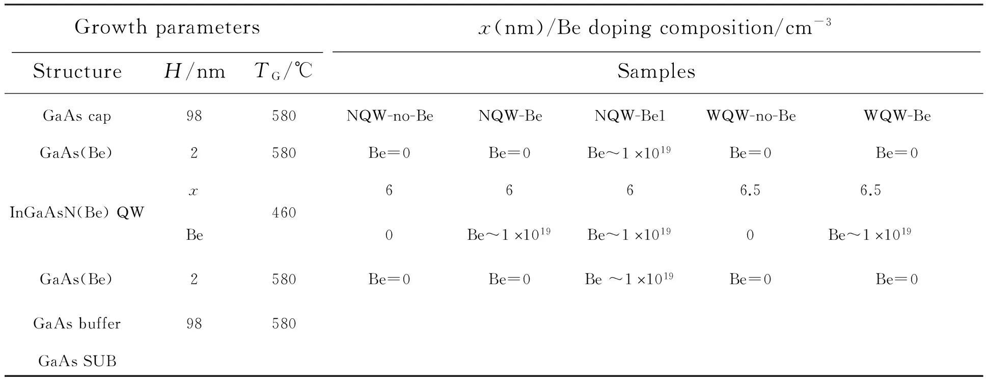
Fig.1 shows the effects of annealing on integrated PL intensities for the QWs with and without Be dopant. The wavelengths of samples of “NQW-Be (RTA)”, “NQW-no-Be (RTA)”, “NQW-Be (as-grown)”, and “NQW-no-Be (as-grown)” were 1 251, 1 228, 1 315, 1 267 nm, respectively. After 50 min of annealing, the PL wavelength of the sample “NQW-Be (RTA)” was longer than that of “NQW-no-Be (RTA)”. The relative peak intensities were 2.57, 0.24, 0.13, and 0.04, respectively. For the as-grown case, the Be doping increased the PL intensity about 3 times, while for 50 min of annealing at 700 ℃, the Be doping increased the PL intensity more than 10 times.
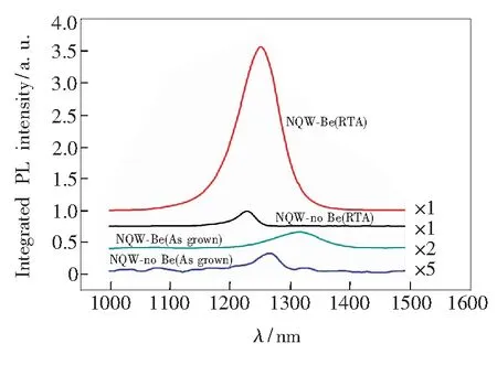
Fig.1 PL spectra of the NQW-series for as-grown and 50 min of RTA at 700 ℃
The lattice structure change during the RTA was evaluated by XRD. The XRD (004) rocking curves of samples “NQW-no-Be” and “NQW-Be” in Fig.2 revealed that the QW peak moves closer to the GaAs substrate peak upon annealing. Annealing introduced larger lattice strain relaxation in QWs without Be-dopant than with Be-dopant due to the high strain inside the QWs. For the as-grown cases, the XRD rocking curves of both samples “NQW-no-Be” and “NQW-Be” fitted exactly each other indicates that the Be dopant didn’t affect the lattice structure during the growth.
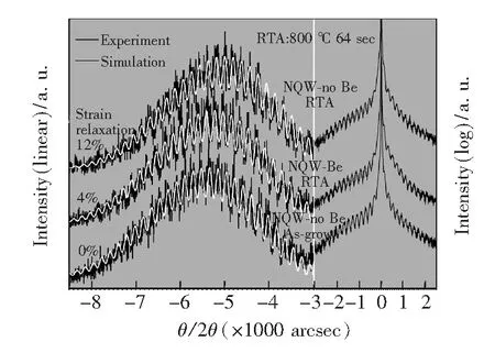
Fig.2 XRD (004) rocking curves for NQW-series before and after 64 s of RTA at 800 ℃ and the strain relaxation simulations (white solid lines) for these curves. For the as-grown cases, the XRD rocking curves of both samples “NQW-no-Be” and “NQW-Be” fitted exactly each other so that only that of the sample “NQW-no-Be” is shown in this figure.
According to the significant improvement of the optical properties and strain relaxation suppression by Be doping, we suggest the following possible physics models: (1) Be doping passivated the N-related points defects; (2) Be doping relaxed the local strain in the InGaAsN(Be) layer.
In previous study[22], the nitrogen related point defects density in DN grown by MBE was reported around 1019cm-3. The Be composition here was also around 1019cm-3. Before thermal annealing, most of the Be atoms were at the interstitial sites of the InGaAsN lattices as well as the N-related point defects due to high composition of both nitrogen and beryllium and low growth temperature. Some of the Be atoms bound with interstitial N atoms[23]. Therefore, Be atoms passivated the N-related point defects. This induces that the PL intensity of the QW with Be (“NQW-Be”) was higher than that without Be (“NQW-no-Be”).
There is huge compress strain in the InGaAsN/GaAs QW. The indium atom is much bigger than gallium and induces compress strain in the InGa(N)/GaAs heterostructures. During the thermal annealing of the sample “NQW-no-Be”, the strain in the InGaAsN layer can be easily relaxed by inducing large number of interface mismatch dislocations which act as large number of nonradiative centers. As for the Be-doping samples, Be atoms bound with interstitial N atoms were activated to the substitutional sites and relaxed the local strain instead of inducing lattice dislocation. From Fig.3, the PL of the sample “NQW-no-Be” was decreased rapidly after 65 s of RTA indicates that the compress strain in this sample was relaxed and dislocations were induced. While the PL of the sample “NQW-Be” decreased slowly after 255 s of annealing. This implies that large number of nonradiative centers were removed and the local strain was relaxed by the Be atoms without dislocation induction before 255 s of annealing. Be atoms bound with interstitial N atoms were activated respectively to both group Ⅲ and Ⅴ sites of the InGaAsN lattices to relax the huge local strain[23]because both Be and N atoms are much smaller than In, Ga and As atoms.
The Be composition in the sample “NQW-Be” was limited due to the limited solubility of Be during growth. Due to the Be composition difference, some of the Be near the interface of InGaAsN(Be)/GaAs was diffused out of the QW. To suppress such diffusion, in the sample “NQW-Be1”, the difference of Be composition at the interface of InGaAsN(Be)/GaAs was removed by increasing 2 nm more Be-doping in GaAs layers at the interfaces of InGaAsN-(Be)/GaAs in both sides of the QW (Fig.3). From Fig.3, the PL intensity of the sample “NQW-Be1” was higher than both “NQW-Be” and “NQW-no-Be”. From the PL dependence of the RTA time that the PL intensity of “NQW-Be1” increased rapidly before 255 s of RTA and turned to saturated after that. This indicates that the Be-doping near the interfaces of the InGaAsN(Be)/GaAs QW successfully suppressed the Be diffusing out of the QW and thus improved the optical properties.
Fig.3 PL peak intensity dependence of RTA time at 700 ℃ for samples NQW-No-Be, NQW-Be, and NQW-Be1. Insert shows the Be profiles of the as-grown samples.
To enlarge the effect of Be-doping in the InGaAsN/GaAs QW, two factors were changed: (1) A set of InGaAsN(Be)/GaAs QW samples were grown with thicker (6.5 nm) QW layer (samples “WQW-no-Be” and “WQW-Be”) which indicates larger strain was in the QW and the QW relaxed more easily during the RTA, than those samples used above. (2) The RTA temperature was increased from 700 to 800 ℃. The structure and PL change were much more obvious than the thinner QW samples. It was observed that, even for the Be-doped QW, the XRD rocking curve peak of the QW moved closer to the GaAs main peak (Fig.4) than 6 nm of QWs. The XRD rocking curves showed strain relaxation of the QW without Be was much more than that of the Be-doped QW. For the as-grown cases, the XRD rocking curves of both samples with and without Be were fitted each other as the samples “NQW-no-Be” and “NQW-Be” did. This indicated that the strain was not relaxed for the as-grown cases when the thickness of the QWs increased from 6.0 to 6.5 nm. The PL from the QW without Be (sample “WQW-no-Be”) reached its maximum in a few seconds time of annealing at 800 ℃ and then decreased quickly and saturated at a level lower than the as-grown case. While, for sample “WQW-Be”, we observed that the PL from the Be-doped QW reached its maximum also in a few seconds but then the decrease rate was smaller than that without Be and increased again after 100 s of annealing and this increasing continued without a saturation even after 900 s of annealing. Fig.5 shows the PL spectra of the two samples (“WQW-no-Be” and “WQW-Be”) after 900 s of annealing at 800 ℃. The wavelengths of the samples “WQW-no-Be” and “WQW-Be” were 1 131 nm and 1 154 nm, respectively. The PL peak intensity of “WQW-Be” was about 80 times higher than “WQW-no-Be” after annealing.
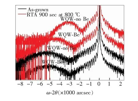
Fig.4 XRD (004) rocking curves for the WQW-series before (black solid lines) and after (red solid lines) 900 s of RTA at 800 ℃ without Be (sample “WQW-Be”) and with Be (sample “WQW-no-Be”). Notice a large shift of non-Be QW diffraction towards the GaAs substrate peak, as opposed to a small shift for Be-doped QW.
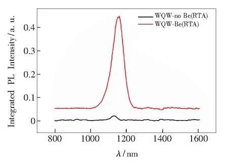
Fig.5 PL spectra of the WQW-series for 900 s of RTA at 800 ℃
4 Conclusion
There are large number of defects in the dilute nitride materials due to low growth temperature and N-plasma radiation. Large strain is required to produce good carrier confinement in the QWs. The doping of Be in the dilute nitride InGaAsN/GaAs QW passivates the point defects and improves the optical properties significantly. The doping of Be also relaxes the local strain without inducing mismatch dislocation and suppresses the dislocations during thermal treatment. Be-doping near the interfaces of the InGaAsN(Be)/GaAs QW successfully suppressed the Be diffusing out of the QW and thus improved the optical properties.
[1] HARRIS J S JR. GaInNAs long-wavelength lasers: progress and challenges [J].Semicond.Sci.Technol., 2002, 17(8):880-891.
[2] KONDOW M, UOMI K, NIWA A,etal.. GaInNAs: a novel material for long-wavelength-range laser diodes with excellent high-temperature performance [J].Jpn.J.Appl.Phys., 1996, 35(2B):1273-1275.
[3] LAAKSONEN K, KOMSA H P, AROLA E,etal.. Computational study of GaAs1-xNxand GaN1-yAsyalloys and arsenic impurities in GaN [J].J.Phys.Condens.Matter, 2006, 18(44):10097-10114.

[5] SCHIRES K, AL SEYAB R, HURTADO A,etal.. Optically-pumped dilute nitride spin-VCSEL [J].Opt.Express, 2012, 20(4):3550-3555.
[6] CARRON R, FEKETE D, GALLO P,etal.. Dilute nitride InGaAsN/GaAs V-groove quantum wires emitting at 1.3 μm wavelength at room temperature [J].Appl.Phys.Lett., 2011, 99(10):101107-1-3.
[7] KLANGTAKAI P, SANORPIM S, ONABE K. Optical study of GaAsN/GaAs and InGaAsN/GaAs T-shaped quantum wires grown by MOVPE [J].J.Cryst.Growth, 2013, 370:200-203.
[8] GLADYSIEWICZ M, KUDRAWIEC R, WARTAK M S. Electronic band structure and material gain of dilute nitride quantum wells grown on InP substrate [J].IEEEJ.Quant.Electron., 2015, 51(5):7100212.
[9] PENG C S, LAINE N, KONTTINEN J,etal.. High-performance singlemode InGaNAs/GaAs laser [J].Electron.Lett., 2004, 40(10):604-605.
[10] ZHAO H, XU Y Q, NI H Q,etal.. Application of rapid thermal annealing on 1.3-1.55 μm GaInNAs(Sb) lasers grown by molecular beam epitaxy [J].J.Cryst.Growth, 2007, 301-302:979-983.
[11] DIMROTH F, GRAVE M, BEUTEL P,etal.. Wafer bonded four-junction GaInP/GaAs//GaInAsP/GaInAs concentrator solar cells with 44.7% efficiency [J].Prog.Photovolt.Res.Appl., 2014, 22(3):277-282.
[12] CHEN S L, JANSSON M, STEHR J E,etal.. Dilute nitride nanowire lasers based on a GaAs/GaNAs core/shell structure [J].NanoLett., 2017, 17(3):1775-1781.
[13] LANGER F, PERL S, H?FLING S,etal.. Graded band gap GaInNAs solar cells [J].Appl.Phys.Lett., 2015, 106(23):233902-1-5.
[14] PENG C S, PAVELESCU E M, JOUHTI T,etal.. Suppression of interfacial atomic diffusion in InGaNAs/GaAs heterostructures grown by molecular-beam epitaxy [J].Appl.Phys.Lett., 2002, 80(25):4720-4722.
[15] TANSU N, QUANDT A, KANSKAR M,etal.. High-performance and high-temperature continuous-wave-operation 1 300 nm InGaAsN quantum well lasers by organometallic vapor phase epitaxy [J].Appl.Phys.Lett., 2003, 83(1):18-20.
[16] BANK S R, YUEN H B, WISTEY M A,etal.. Effects of growth temperature on the structural and optical properties of 1.55 μm GaInNAsSb quantum wells grown on GaAs [J].Appl.Phys.Lett., 2005, 87(2):021908-1-3.
[17] FAN W J, BOSE S, ZHANG D H. Electronic bandstructure and optical gain of lattice matched Ⅲ-Ⅴ dilute nitride bismide quantum wells for 1.55 μm optical communication systems [J].J.Appl.Phys., 2016, 120(9):093111-1-9.
[18] KASANABOINA P K, AHMAD E, LI J,etal.. Self-catalyzed growth of dilute nitride GaAs/GaAsSbN/GaAs core-shell nanowires by molecular beam epitaxy [J].Appl.Phys.Lett., 2015, 107(10):103111-1-3.
[19] JANOTTI A, REUNCHAN P, LIMPIJUMNONG S,etal.. Mutual passivation of electrically active and isovalent impurities in dilute nitrides [J].Phys.Rev.Lett., 2008, 100(4):045505-1-4.
[20] YU K M, WALUKIEWICZ W, WU J,etal.. Mutual passivation of electrically active and isovalent impurities [J].Nat.Mater., 2002, 1(3):185-189.
[21] PAKARINEN J, PENG C S, PUUSTINEN J,etal.. Postgrowth annealing of GaInAs/GaAs and GaInAsN/GaAs quantum well samples placed in a proximity GaAs box: a simple method to improve the crystalline quality [J].Appl.Phys.Lett., 2008, 92(23):232105-1-4.
[22] PENG C S, LI W, JOUHTI T,etal.. A study and control of lattice sites of N and In/Ga interdiffusion in dilute nitride quantum wells [J].J.Cryst.Growth, 2003, 251(1-4):378-382.
[23] KOMSA H P, AROLA E, PAKARINEN J,etal.. Beryllium doping of GaAs and GaAsN studied from first principles [J].Phys.Rev. B, 2009, 79(11):115208-1-9.

霍大云(1988-),男,安徽當涂人,博士生研究生,2012年于淮北師范大學獲得學士學位,主要從事半導體量子點的研究。
E-mail: huodayun@126.com彭長四(1966-),男,湖南漣源人,博士,教授,1998年于中科院北京物理所獲得博士學位,2009年于芬蘭坦佩雷科技大學獲得博士學位(在職),主要從事半導體量子點、納米仿生和太陽能電池等方面的研究。
E-mail: changsipeng@suda.edu.cn
2017-01-19;
2017-03-13
國家自然科學基金 (11504251,51302179); 江蘇高校優勢學科建設工程; 科技部國際合作項目(2013DFG12210); 江蘇省高校自然科學研究重大項目(12KJA140001); 江蘇省普通高校研究生科研創新計劃(KYLX15_1252)資助項目 Supported by National Natural Science Foundation of China (91323303, 11504251); Priority Academic Program Development of Jiangsu Higher Education Institutions (PAPD); International Cooperation Project by MOST (2014DFG12600); Natural Science Research Project of Jiangsu Higher Education (13KJA510006); Research Plan of Graduate Students in Jiangsu Province (KYLX15_1252)
Be摻雜對InGaAsN/GaAs量子阱性能的提高
霍大云1,2, 石震武1,2, 徐 超1,2, 鄧長威1,2, 陳 晨1,2,陳林森1,2, 王文新3, 彭長四1,2*
(1. 蘇州大學 光電信息科學與工程學院, 蘇州納米科技協同創新中心, 江蘇 蘇州 215006; 2. 蘇州大學 江蘇省先進光學技術重點實驗室, 教育部現代光學技術重點實驗室, 江蘇 蘇州 215006; 3. 中國科學院物理研究所 北京凝聚態物理國家實驗室, 北京 100190)
InGaAsN/GaAs量子阱中進行鈹(Be)元素重摻雜能顯著提高其光學性質,并且發光波長發生了紅移。X射線衍射搖擺曲線清楚地證實了鈹摻雜抑制了InGaAsN(Be)/GaAs量子阱在退火過程中的應力釋放。對比退火前,退火后的沒有進行鈹摻雜的量子阱樣品的量子阱的X射線搖擺曲線衍射峰明顯向GaAs襯底峰偏移;而對于摻鈹的量子阱樣品而言,這樣的偏移要小很多。
稀氮化物; 分子束外延; 量子阱; 應變弛豫; X射線衍射
1000-7032(2017)08-1056-07
O484.4 Document code: A
10.3788/fgxb20173808.1056
猜你喜歡
電子競技(2020年8期)2020-12-23 04:09:40
電子競技(2020年7期)2020-10-12 10:45:48
電子競技(2020年5期)2020-08-10 08:43:10
電子競技(2020年4期)2020-07-13 09:18:06
電子競技(2020年2期)2020-04-14 04:40:38
電子競技(2020年11期)2020-02-07 02:49:36
電子競技(2020年9期)2020-01-11 01:06:21
電子競技(2020年10期)2020-01-11 01:06:06
電子競技(2019年22期)2019-03-07 05:17:26
電子競技(2019年21期)2019-02-24 06:55:52
