激基復合物給體作間隔層對激子復合區域的調節
2017-04-12 08:54:34高浩鋒方圣歡張葉峰呂昭月
發光學報 2017年4期
高浩鋒, 方圣歡, 張葉峰, 陸 勍, 呂昭月
(華東理工大學理學院 物理系, 上海 200237)
激基復合物給體作間隔層對激子復合區域的調節
高浩鋒, 方圣歡, 張葉峰, 陸 勍, 呂昭月*
(華東理工大學理學院 物理系, 上海 200237)
為研究激基復合物器件激子復合區域的變化,在TPD/BPhen界面可形成激基復合物發光的基礎上,以Ir(pq)2(acac)為探測層,制備器件ITO/MoO3(2.5 nm)/TPD((40-x) nm)/Ir(pq)2(acac)(0.5 nm)/TPD(x,x=0,3,6,10 nm)/BPhen(40 nm)/Cs2CO3/Al,其中靠近BPhen的TPD稱之為間隔層。電致發光光譜表明,該組器件的激子復合區域主要位于Ir(pq)2(acac)薄層和TPD/BPhen界面,分別發射595 nm和478 nm的光。隨著TPD間隔層厚度的增加和電壓的升高,發光區域向激基復合物區域(TPD/BPhen界面)移動,即更多的電子和空穴在TPD/BPhen界面形成激基復合物發光,Ir(pq)2(acac)發光減弱。當間隔層厚度由0 nm增至10 nm時,6 V電壓下的Ir(pq)2(acac)和激基復合物發光強度的比值由44降至1.5。對于間隔層厚度為6 nm的器件,Ir(pq)2(acac)和激基復合物發光強度的比值由6 V時的2.8降至10 V時的1.0。由此可見,激基復合物給體作間隔層能有效調節激子復合區域。
間隔層; 激基復合物; 激子復合區域; TPD; BPhen
1 引 言
有機發光二極管(Organic light-emitting diode,OLED)因其平板化、響應速度快、驅動電壓低、高亮度、面發光等優點在顯示、照明領域具有極大的應用空間[1-4]。經過近三十年的發展,其效率及壽命已得到了極大的改善,目前在顯示領域已占有一定的市場份額,很多性能已超越液晶顯示器。但是,OLED仍存在一些問題需要解決,如產業化過程中大規模生產工藝及成本控制等技術問題、使用壽命短(穩定性差)、顏色變化(即激子復合區域的變化)、發光效率及衰減機理等基本科學問題。本文側重研究關于激子復合區域的科學問題。
作為雙載流子注入型器件,OLED中的激子復合受載流子的注入、傳輸的影響,通過設計合理的器件結構能控制其激子復合區域。其中,使用間隔層是一種簡單、有效的方法[5-8]。黃晉等[7]以BCP (Bathocuproine)作為間隔層調節紅色磷光器件的載流子復合,使其色坐標穩定在(0.643,0.353)左右,且不隨電壓變化而改變。李懷坤等[8]使用BPhen (4,7-diphenyl-1,10-phenanthroline)作為發光層間隔層調節激子復合區域,發現引入適當厚度的BPhen間隔層可以有效地遏制器件激子復合區域隨電壓增大而漂移[9],使器件的色坐標相對穩定。
除上述電子傳輸材料作為間隔層外,其他類型的間隔層材料也能有效控制激子復合區域,如空穴傳輸材料NPB(N,N′-diphenyl-N,N′-bis(1-naphthyl-phenyl)-1,1′-biphenyl-4,4′-diamine)[10-11]、雙極性電荷傳輸材料CBP(N,N′-dicarbazolyl-4,4′- biphenyl)[12]、電子傳輸與空穴傳輸混合材料(CBP∶BPhen)[13]。采用間隔層調控激子復合物區域,我們已取得一些研究結果,不僅能夠調節常規發光體的復合區域[5-6],也能有效調控電致激基復合物器件的復合區域并改善器件的色穩定性[14]。然而,目前間隔層還很少被應用于激基復合物OLED器件中。
所謂激基復合物是一種分子激發態與另一種分子基態的相互作用,常在OLED的空穴傳輸材料和電子傳輸材料的界面處形成。激基復合物發光會使OLED光譜紅移和展寬,可用于調節光譜和制作白光器件[15-16]。由于其發光效率低,影響OLED的色穩定性及效率[17],早期的研究認為應避免其產生。然而近年來的研究表明:(1) 激基復合物作為磷光主體材料,可以充分利用其三重態能量,獲得高效率的OLED[18];(2) 激基復合物容易實現熱激活延遲熒光(Thermally activated delayed fluorescence,TADF),使三重態逆系間竄越(Reverse intersystem crossing,RISC)至單重態,理論上通過TADF可在熒光材料體系中實現100%的內量子效率[19-20]。因此激基復合物再一次受到研究人員的青睞。
本文以激基復合物器件ITO/MoO3/TPD/BPhen/Cs2CO3/Al為基礎,其中TPD(N,N′-bis(3-methylphenyl)-N,N′-bis(phenyl)-benzidine)為激基復合物給體,BPhen是受體,采用給體TPD作間隔層制備了器件 ITO/MoO3/TPD((40-x) nm)/Ir(pq)2(acac)(0.5 nm)/TPD(x,x=0,3,6,10 nm)/BPhen/Cs2CO3/Al。基于Ir(pq)2(acac) (Bis(2-phenylpyridine) iridium(Ⅲ) acetylacetonate)探測層,通過分析其電致發光光譜(Electroluminescent,EL)研究了給體TPD間隔層對激基復合物器件載流子復合區域的影響。
2 實 驗
2.1 材料
ITO導電玻璃購自深圳華南湘城科技有限公司,MoO3購自百靈威科技有限公司,TPD、BPhen、Ir(pq)2(acac)均購自上海瀚豐化工科技有限公司,Cs2CO3購自Sigma Aldrich公司,金屬Al購于中諾新材(北京)科技有限公司。有機材料的分子結構如圖1所示。
2.2 器件制備
為研究激基復合物給體作間隔層對激子復合區域的影響,本實驗以激基復合物器件ITO/MoO3(2.5 nm)/TPD(40 nm)/BPhen(40 nm)/Cs2CO3/Al為基礎,采用給體TPD為間隔層,制備了器件ITO/MoO3(2.5 nm)/TPD1((40-x) nm)/Ir(pq)2(acac)(0.5 nm)/TPD2(x,x=0,3,6,10 nm)/BPhen(40 nm)/Cs2CO3(1.5 nm) /Al,并將x=0,3,6,10 nm的器件分別命名為器件Ⅰ~Ⅳ。器件結構如圖2所示。為方便區別,將靠近陽極的TPD層稱為TPD1,靠近BPhen的TPD(間隔層)稱為TPD2。
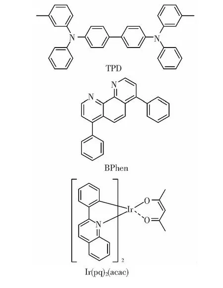
圖1 實驗所用有機材料的分子結構
Fig.1 Molecular structures of organic materials used in the experiment
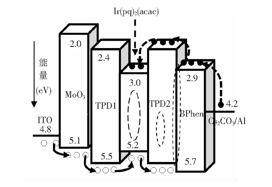
圖2 器件結構及能級排列圖,其中空心圓代表空穴,實心圓代表電子,虛線橢圓代表復合區域。
Fig.2 Diagram of device structure and energy levels alignment (open circles are holes, solid circles are electrons; and dashed ovals are recombination zone)
蒸鍍前,對ITO導電玻璃基片進行常規清洗:先把基片放入60 ℃水浴中浸泡10 min,再依次放入去離子水、無水乙醇和異丙醇溶液中超聲清洗,然后用壓縮空氣吹干,最后進行氧等離子處理。處理好的ITO基片放入立寧真空LN-386SA 型多源有機分子氣相沉積系統中順序蒸鍍各功能層。蒸鍍時,蒸鍍室的真空度保持在5×10⁻⁴Pa以下,并用 6 MHz的石英晶振膜厚儀監測薄膜的沉積速率和厚度。
2.3 性能測試
器件的光電性能(電致發光光譜以及電流-電壓-亮度-效率特性)由軟件控制的Keithley 2400電源和柯尼卡美能達CS2000分光光度計測得。所有測量均在室溫大氣環境下進行。
3 結果與討論
首先討論TPD/BPhen界面激基復合物的形成。圖3所示是器件ITO/TPD/BPhen/Cs2CO3/Al不同電壓下的電致發光光譜,圖中顯示光譜有400 nm和478 nm兩個峰。根據Zhu等的報道,TPD和BPhen的發光峰分別位于400 nm[21-22]和380 nm左右[22-23],也就是說,圖3中400 nm的發光來自TPD,而478 nm既不是TPD的發光也不是BPhen的發光。
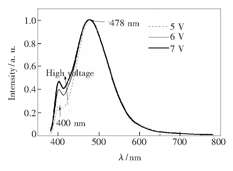
圖3 ITO/TPD/BPhen/Cs2CO3/Al的歸一化光譜
Fig.3 Normalized spectra of ITO/TPD/BPhen/Cs2CO3/Al
經計算[24],478 nm的光子能量為2.6 eV,與圖2中TPD的HOMO能級與BPhen的LUMO能級差相吻合,結合Wu等的報道[23],可以推斷478 nm的發光峰來自TPD/BPhen界面形成的激基復合物發光。圖3還表明隨著電壓的升高,TPD的發光逐漸增強。原因是激基復合物的熒光量子效率較低,當堆積于界面的電子和空穴較多時,電子、空穴不能全部轉化為激基復合物發光,部分進入TPD分子復合發光。
圖4是器件Ⅰ~Ⅳ在不同電壓(6,8,10 V)下的電致發光光譜。從圖中可以看出,4個器件主要有兩個發光峰 (478,595 nm),分別來自TPD/BPhen界面激基復合物和Ir(pq)2(acac)的發光。根據圖2中器件的能級排列,Ir(pq)2(acac)在器件中形成了能級陷阱,捕獲分別從陰極和陽極注入的電子和空穴形成激子發射出峰值為595 nm的光[25]。把器件Ⅰ~Ⅳ的發光光譜380~600 nm波段進行放大(圖5),并與器件ITO/TPD/BPhen/Cs2CO3/Al的光譜對比,容易發現器件Ⅰ~Ⅳ中478 nm的發光峰與激基復合物發光吻合。
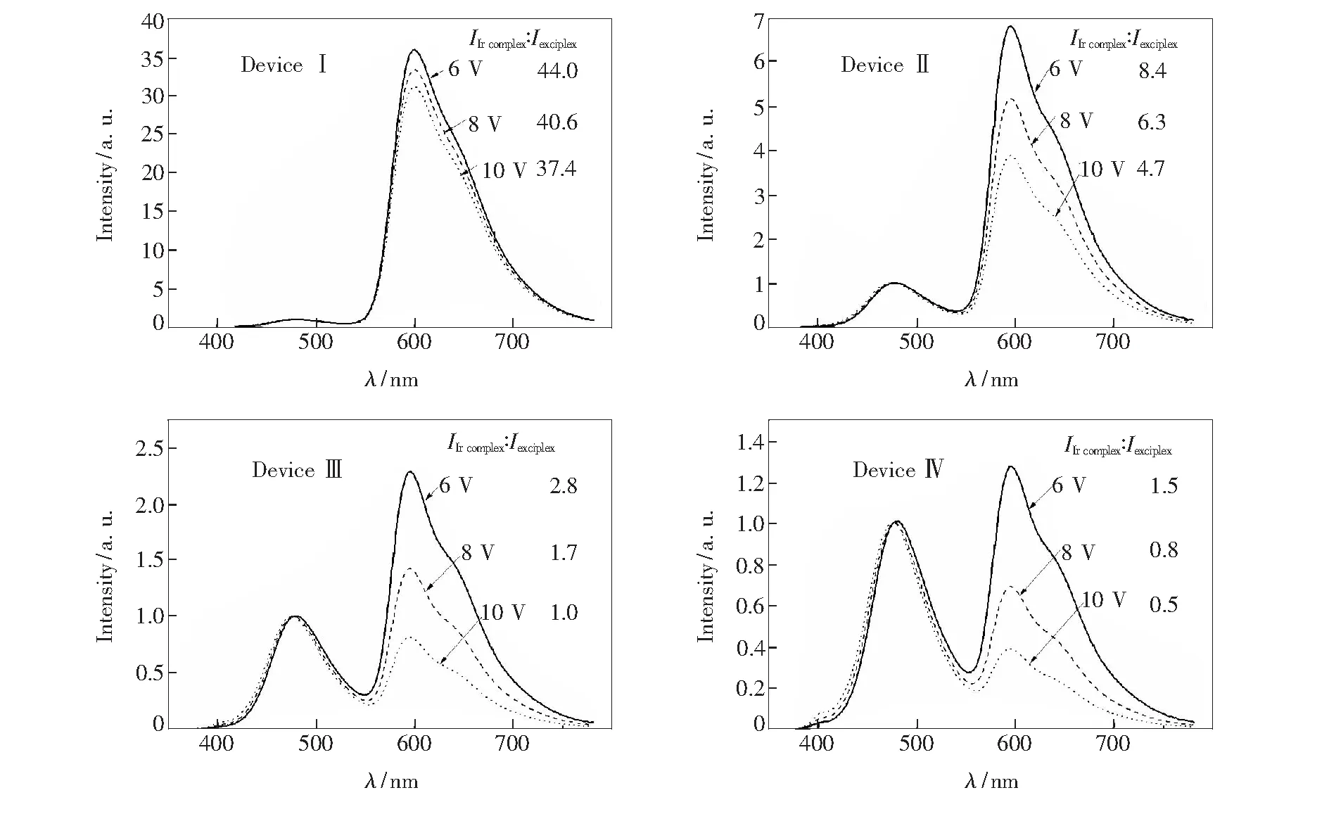
圖4 器件Ⅰ~Ⅳ在不同電壓下的電致發光光譜
同時,隨著TPD2厚度的增加,Ir(pq)2(acac)的相對發光強度(IIr complex)逐漸減小。如:6 V電壓下,器件Ⅰ~Ⅳ(分別對應間隔層厚度0,3,6,10 nm)中的IIr complex∶Iexciplex的值分別為44.0,8.4,2.8,1.5,其中,Iexciplex代表激基復合物的發光強度。這里,計算光強時,認為器件的光譜是Ir(pq)2(acac)和TPD/BPhen激基復合物發光的線性疊加,簡單地對光譜進行分解,得到Ir(pq)2-(acac)和激基復合物的光譜,相應的發光強度是各分解光譜的積分。后文中無特別說明,計算方法與此相同。因為間隔層TPD2厚度的增加,電子更難越過TPD/BPhen的界面勢壘進入Ir(pq)2-(acac),更多的電子積聚在TPD/BPhen的界面處,與同樣聚集在該界面的空穴形成激基復合物發光。此外,隨著TPD2厚度的增加,由于TPD/BPhen界面處堆積的電子和空穴不能全部轉化為激基復合物發光,繼而轉入TPD中發光,400 nm 發光峰逐漸凸顯出來。
圖4還表明IIr complex∶Iexciplex隨著電壓的增大而減小。器件Ⅰ中,由于Ir(pq)2(acac)的厚度僅有0.5 nm,非常薄,TPD與BPhen仍部分相互接觸形成界面,從而產生激基復合物發光。隨著電壓的增大,當Ir(pq)2(acac)的發光達到飽和后,其余的電子和空穴在TPD/BPhen界面發光,使得Ir(pq)2(acac)發光相對減弱。在器件Ⅱ~Ⅳ中,電子從TPD/BPhen界面進入Ir(pq)2(acac)需要越過0.5 eV的能級勢壘,而空穴從Ir(pq)2(acac)陷阱到TPD/BPhen的界面僅需越過0.3 eV的勢壘,因此隨著電壓的增大,被陷阱所捕獲的空穴更容易逃逸進入TPD,并與堆積于TPD/BPhen界面處的電子形成激基復合物發光,使得激基復合物的發光相對增強。
圖6和7分別是器件Ⅰ~Ⅳ的電流密度-電壓-亮度特性曲線以及電流效率-電流密度曲線。從圖中可以發現,器件Ⅰ~Ⅳ的電流密度幾乎不變,即間隔層(TPD2)的厚度基本不影響載流子的注入和傳輸,但對于發光亮度和效率的影響很大。隨著TPD2厚度的增加,激子復合區域向TPD/BPhen界面處移動,界面處激基復合物的發光量子產率遠低于Ir(pq)2(acac),因此器件的亮度以及發光效率有所下降。同時,效率衰減(Efficiency roll-off)也因激子復合區域變化而改變:當光譜中Ir(pq)2-(acac)的發光所占比例較大時(器件Ⅰ和Ⅱ),由于高電流密度下磷光材料Ir(pq)2(acac)中的三重態-三重態湮滅導致效率衰減很快;對應地,當激基復合物發光強度增加時(器件Ⅲ和Ⅳ),效率衰減相對緩慢。
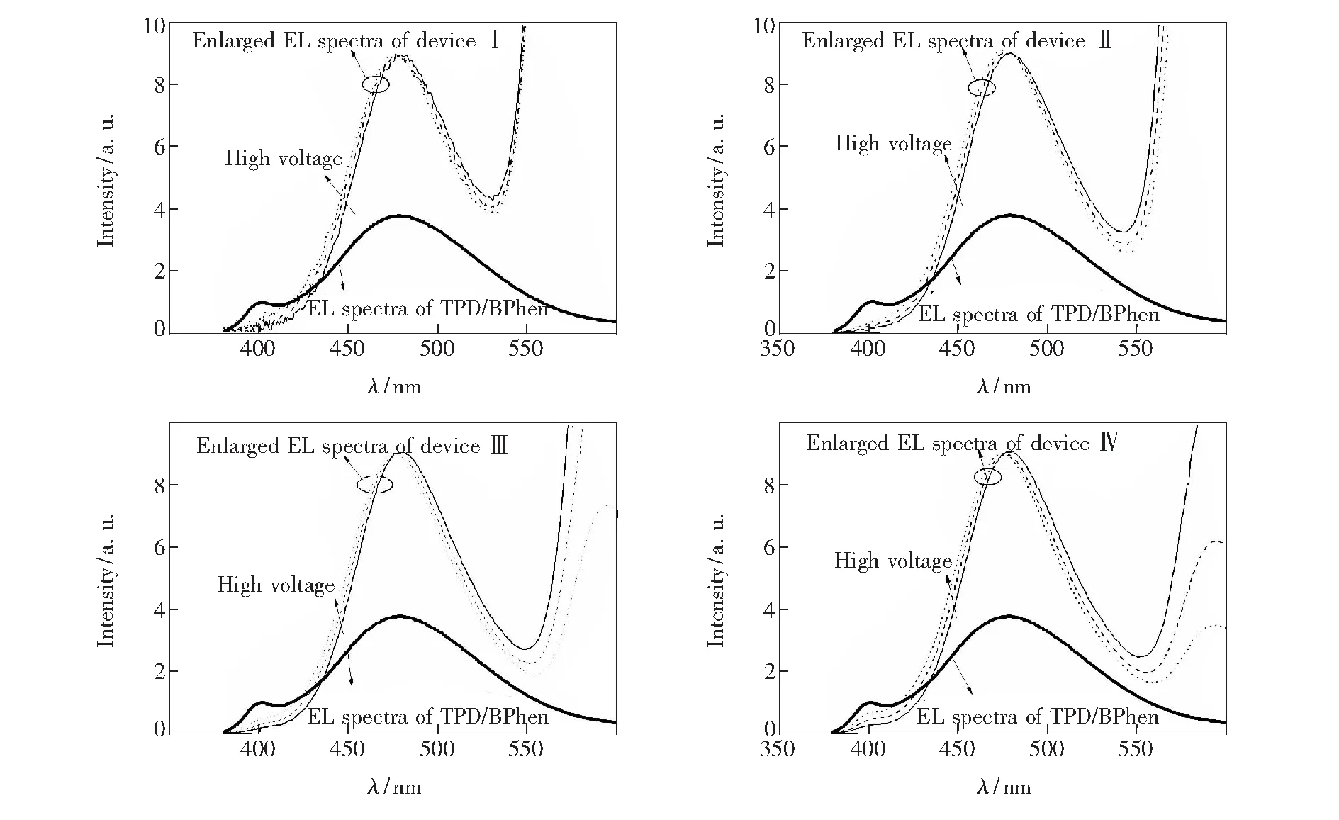
圖5 器件Ⅰ~Ⅳ的激基復合物光譜分析
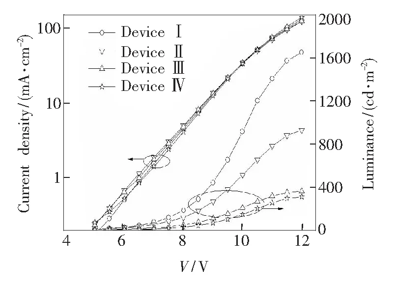
圖6 器件Ⅰ~Ⅳ的電流密度-電壓-亮度曲線
Fig.6 Current density-voltage-luminance curves of devicesⅠ-Ⅳ
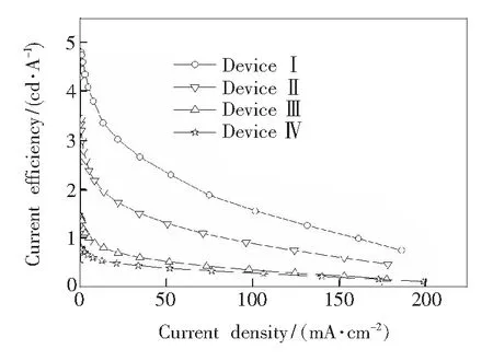
圖7 器件Ⅰ~Ⅳ的電流效率-電流密度曲線
Fig.7 Current efficiency-current density plots of device Ⅰ-Ⅳ
4 結 論
基于TPD/BPhen界面形成激基復合物,本文以激基復合物給體TPD作為間隔層,采用Ir(pq)2(acac)作為探測層研究間隔層厚度對激基復合物OLED中激子復合區域及光電性能的調節。在6 V電壓下,在TPD間隔層為0,3,6,10 nm的器件中,探測層Ir(pq)2(acac)和TPD/BPhen界面激基復合物的發光強度之比(IIr complex∶Iexciplex)分別為44.0,8.4,2.8,1.5。隨TPD間隔層厚度的增加,更多載流子在TPD/BPhen界面復合形成激基復合物發光。當TPD間隔層厚度為3 nm時,IIr complex∶Iexciplex在6,8,10 V電壓下分別為8.4,6.3,4.7,隨著電壓的升高,復合區域也向TPD/BPhen界面移動(TPD間隔層厚度為0,6,10 nm時也表現同樣的趨勢)。上述結果表明,在激基復合物器件中,采用激基復合物給體作間隔層能有效控制激子復合區域,調節器件的發光顏色。尤其是顏色隨電壓的變化可考慮應用于視覺隱身技術。
[1] TANG C W, VANSLYKE S A. Organic electroluminescent diodes [J].Appl.Phys.Lett., 1987, 51:913-915.
[2] KIM K H, PARK S Y. Enhancing light-extraction efficiency of OLEDs with high- and low-refractive-index organic-inorganic hybrid materials [J].Org.Electron., 2016, 36:103-112.
[3] YAMADA S, SHIM C H, EDURA T,etal.. Fabrication of bottom-emitting organic light-emitting diode panels interconnected with encapsulation substrate by Au-Au flip-chip bonding and capillary-driven filling process [J].Microelectron.Eng., 2016, 161:94-97.
[4] SUN Q J, FAN B H, TAN Z A,etal.. White light from polymer light-emitting diodes: utilization of fluorenone defects and exciplex [J].Appl.Phys.Lett., 2016, 88(16):163510-1-3.
[5] Lü Z Y, HOU Y, XIAO J,etal.. Emission spectra dependence on voltage and emissive layer layout in organic light-emitting diodes [J].Vacuum, 2014, 109:197-199.
[6] Lü Z Y, HOU Y, XIAO J,etal.. Effects of emissive layer architecture on recombination zone and F?rster resonance energy transfer in organic light-emitting diodes [J].Displays, 2014, 35(5):247-251.
[7] 黃晉, 張方輝. BCP對紅色有機電致磷光器件效率的影響 [J]. 光譜學與光譜分析, 2013, 33(7):1767-1770. HUANG J, ZHANG F H. Influence of BCP on efficiency of red phosphorescent electroluminescent device [J].Spectrosc.Spectr.Anal., 2013, 33(7):1767-1770. (in Chinese)
[8] 李懷坤, 張方輝, 程君, 等. BPhen作為發光層間隔層對黃光OLED的影響 [J]. 發光學報, 2016, 37(1):38-43. LI H K, ZHANG F H, CHENG J,etal.. Effects of BPhen as spacer layer in light emitting layer on yellow OLED [J].Chin.J.Lumin., 2016, 37(1):38-43. (in Chinese)
[9] SEO Y S, MOON D G. Recombination zone shift in phosphorescent white organic light-emitting devices with single host structure of multi-emission layers [J].Curr.Appl.Phys., 2014, 14(9):1188-1191.
[10] HO C L, WONG W Y, WANG Q,etal.. A multifunctional iridium-carbazolyl orange phosphor for high-performance two-element WOLED exploiting exciton-managed fluorescence/phosphorescence [J].Adv.Funct.Mater., 2008, 18(6):928-937.
[11] YAN B P, CHEUNG C C C, KUI S C F,etal.. Efficient white organic light-emitting devices based on phosphorescent platinum(Ⅱ)/fluorescent dual-emitting layers [J].Adv.Mater., 2007, 19(21):3599-3603.
[12] CHEN P, XIE W F, LI J,etal.. White organic light-emitting devices with a bipolar transport layer between blue fluorescent and orange phosphorescent emitting layers [J].Appl.Phys.Lett., 2007, 91:023505.
[13] WANG Y, HUA Y L, WU X M,etal.. Application of mixed interface in white-electrophosphorescent devices: an efficient approach to adjust the distributions of carriers [J].Appl.Phys.Lett., 2008, 93:113302.
[14] Lü Z Y, YIN Y H, XIAO J. Manipulation of recombination zone by utilizing the donor of electroplex as a spacer [J].J.Lumin., 2016, 179:469-473.
[15] 李雪蓮, 駱開均, 李祥龍, 等. 新型藍色熒光材料5,5′,6,6′-四苯基-2,2′-聯吡嗪的制備和發光性質 [J]. 發光學報, 2016, 37(3):257-264. LI X L, LUO K J, LI X L,etal.. Synthesis and luminescence of new blue fluorescent 5,5′,6,6′-tetraphenyl-2,2’-bipyrazine [J].Chin.J.Lumin., 2016, 37(3):257-264. (in Chinese)
[16] KALINOWSKI J, COCCI M, VIRGILI D,etal.. Mixing of excimer and exciplex emission: a new way to improve white light emitting organic electrophosphorescent diodes [J].Adv.Mater., 2007, 19(22):4000-4005.
[17] MATSUMOTO N, NISHIYAMA M, ADACHI C. Exciplex formations between Tris(8-hydoxyquinolate)aluminum and hole transport materials and their photoluminescence and electroluminescence characteristics [J].J.Phys.Chem. C, 2008, 112(20):7735-7741.
[18] PARK Y S, KIM K H, KIM J J. Efficient triplet harvesting by fluorescent molecules through exciplexes for high efficiency organic light-emitting diodes [J].Appl.Phys.Lett., 2013, 102(15):153306-1-5.
[19] LI J, NOMURA H, MIYAZAKI H,etal.. Highly efficient exciplex organic light-emitting diodes incorporating a heptazine derivative as an electron acceptor [J].Chem.Commun., 2014, 50(46):6174-6176.
[20] CHEN D C, WANG Z H, WANG D,etal.. Efficient exciplex organic light-emitting diodes with a bipolar acceptor [J].Org.Electron., 2015, 25:79-84.
[21] ZHU H N, XU Z, ZHANG F J,etal.. Exciplex or electroplex emissions from the interface between aromatic diamine and 2,9-dimethyl-4,7-diphenyl-1,10-phenanthroline? [J].Appl.Surf.Sci., 2008, 254(17):5511-5513.
[22] ZHU J Z, LI W L, HAN L L,etal.. Very broad white-emission spectrum based organic light-emitting diodes by four exciplex emission bands.[J].Opt.Lett., 2009, 34(19):2946-2948.
[23] WU W, LI F S, NIE C,etal.. Improved performance of flexible white hybrid light emitting diodes by adjusting quantum dots distribution in polymer matrix [J].Vacuum, 2015, 111:1-4.
[24] NAUENBERG M. The evolution of radiation toward thermal equilibrium: a soluble model that illustrates the foundations of statistical mechanics [J].Am.J.Phys., 2004, 72(3):313-323.
[25] LAI C C, HUANG M J, CHOU H H,etal..m-Indolocarbazole derivative as a universal host material for RGB and white phosphorescent OLEDs [J].Adv.Funct.Mater., 2015, 25(34):5548-5556.

高浩鋒 (1995-),男,浙江上虞人,華東理工大學本科生,主要從事有機光電子器件的研究。

E-mail: 10141692@mail.ecust.edu.cn呂昭月(1983-),女,云南鎮雄人,博士,講師,2012年于北京交通大學獲得博士學位,主要從事有機光電子器件的研究。
E-mail: lvzhaoyue@ecust. edu.cn
Adjustment of Exciton Recombination Zone by Utilizing The Donor of Exciplex as Spacer Layer
GAO Hao-feng, FANG Sheng-huan, ZHANG Ye-feng, LU Qing, LYU Zhao-yue*
(DepartmentofPhysics,SchoolofScience,EastChinaUniversityofScienceandTechnology,Shanghai200237,China)*CorrespondingAuthor,E-mail:lvzhaoyue@ecust.edu.cn
In order to adjust the exciton recombination zone of exciplex-based organic light-emitting diodes, four devices were fabricated by employing Ir(pq)2(acac) as a prober and utilizing the donor of exciplex as a spacer. The device structures are ITO/MoO3(2.5 nm)/TPD((40-x) nm)/Ir(pq)2(acac)(0.5 nm)/TPD(x,x=0, 3, 6, 10 nm)/BPhen(40 nm)/Cs2CO3/Al, wherexis the thickness of the spacer layer and the TPD/BPhen interface produces the exciplex emission. The electroluminescent spectra of the four devices include two main peaks: 478 nm and 595 nm, which originate from the TPD/BPhen interface and Ir(pq)2(acac) layer , respectively. As both the thickness of TPD spacer and the applied voltage increase, the recombination zone shifts towards TPD/BPhen interface. That is, more electrons and holes recombine at the interface between TPD and BPhen, leading to the decreased intensity of Ir(pq)2(acac) emission. For instance, under an applied voltage of 6 V, the intensity ratio of emission from Ir(pq)2(acac) and exciplex (IIr complex∶Iexciplex) is 44.0 and 1.5 for the devices with 0 and 10 nm spacer, respectively. The value ofIIr complex∶Iexciplexdecreases from 2.8 at 6 V to 1.0 at 10 V for the device with 6-nm-thick TPD spacer. Therefore, the recombination region can be effectively tuned by utilizing the donor of exciplex as a spacer.
spacer; exciplex; exciton recombination zone; TPD; BPhen
2016-10-25;
2016-11-25
國家自然科學基金(11504109); 上海市大學生創新訓練項目(S16089)資助 Supported by National Natural Science Foundation of China (11504109); College Students Innovation Training Program of Shanghai (S16089)
1000-7032(2017)04-0514-07
TN383+.1
A
10.3788/fgxb20173804.0514
猜你喜歡
今日農業(2021年9期)2021-11-26 07:41:24
發明與創新·小學生(2021年3期)2021-03-25 11:48:49
當代陜西(2020年13期)2020-08-24 08:22:02
制造技術與機床(2017年5期)2018-01-19 02:49:17
金秋(2017年4期)2017-06-07 08:22:16
中國材料進展(2016年10期)2016-12-26 06:50:20
濰坊學院學報(2016年2期)2016-12-01 13:00:11
中國科技博覽(2016年2期)2016-04-25 20:32:39
小學生導刊(2016年34期)2016-04-11 00:49:44
新聞傳播(2015年11期)2015-07-18 11:15:04