GaAs單片二極管雙平衡混頻器
2010-09-05 06:26:50彭龍新1李建平
電子與封裝 2010年9期
陳 坤,彭龍新1,,李建平
(1.單片集成電路與模塊國家重點實驗室,南京 210016;2.南京電子器件研究所,南京 210016)
GaAs單片二極管雙平衡混頻器
陳 坤2,彭龍新1,2,李建平2
(1.單片集成電路與模塊國家重點實驗室,南京 210016;2.南京電子器件研究所,南京 210016)
采用0.25 μm的GaAs工藝制作了一款單片二極管雙平衡混頻器。基于環形二極管雙平衡混頻器的基本工作原理,提出了LO巴倫與RF巴倫的區別所在,并以Marchand巴倫為LO巴倫,以triformer巴倫作為RF巴倫。在優化了局部電路后,再與環形二極管組成整體電路,并對整體電路進行了優化。最后對版圖進行EM仿真,并稍作調整以改善EM仿真結果。當本振功率在13dBm時,實測得轉換損耗在低本振和高本振下約為11.5dB和10.5dB,LO端口到IF端口和RF端口隔離度分別為30dB和35dB,LO端口和RF端口駐波分別小于2和3.5,實測結果與仿真結果基本一致。
雙平衡混頻器;環形二極管;巴倫;微波單片集成電路;轉換損耗
1 引言
雙平衡混頻器理論上能夠有效地抑制寄生混頻產物,各端口之間也有很好的隔離,是混頻器設計的優選結構[3,5,6]。其中,二極管環形雙平衡混頻器的結構相對簡單,易于實現,關鍵在于設計具有良好性能的巴倫。在混頻器設計中,一般認為本振(LO)信號幅度遠大于射頻(RF)信號幅度,二極管的導通與截止完全取決于LO信號。所以,從時域角度考慮,LO巴倫處于支配地位,可以使用一般形式的Marchand巴倫[1,2]實現;RF巴倫則處于被支配地位,RF巴倫可由triformer巴倫[4]實現。由于二極管阻抗的非線性,不一定匹配于參考阻抗Z0,故仍需要對整體電路加以優化和調整。以優化后的參數繪制版圖,并對版圖進行EM仿真,最后采用0.25 μm的GaAs工藝制作了電路。當RF與LO頻率為2.5 GHz~5.0GHz、中頻為0.5 GHz~1.5GHz時,實測變頻損耗約為11.5dB,LO到IF和RF的隔離度分別為30dB和35dB,LO和RF端口駐波分別小于2和3.5。
2 電路設計
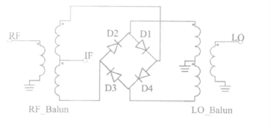
環形二極管雙平衡混頻器原理圖如圖1所示。當LO信號幅度遠大于RF信號幅度時,在LO半周期內D2、D3與D1、D4交替導通,而RF巴倫的兩個輸出端則交替處于開路和導通狀態,同時從RF巴倫的輸出公共端引出I F。據此工作特性,L O巴倫由Marchand巴倫[1]或螺旋變壓器式巴倫[7]實現,本文采用Marchand巴倫結構;RF巴倫由triformer巴倫[4]實現。
RF巴倫的結構圖如圖2(a)所示,線寬、間距及線總長分別取8μm、4μm及3000μm。RF巴倫的輸出特性如圖2(b)所示,顯示了在工作頻帶2.5GHz~5.0GHz內,輸出幅度平衡性小于1dB,相位平衡性小于5°,說明RF巴倫具有良好的平衡特性。
將LO巴倫、RF巴倫以及環形二極管組成完整電路,設置優化參數以及合適的優化目標進行優化,得到雙平衡混頻器的仿真結果如圖3所示。
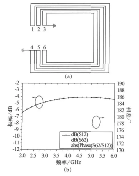
圖2 triformer巴倫(a)結構,(b)輸出特性
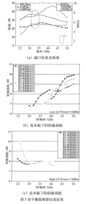
可以看出各端口之間的隔離性極好,其中LO到RF隔離大于25dB,LO到IF隔離大于20dB;LO端口駐波約小于2,RF端口駐波小于3;當本振功率為13dBm時,轉換損耗低于10.5dB,低本振下的轉換損耗優于高本振下的情況。
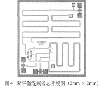
最后將電路模型轉化為版圖,合理地折彎微帶線以減小尺寸,并對版圖中部分參數作適當調整,以使EM仿真也滿足性能要求,芯片的版圖如圖4所示。
3 實測結果
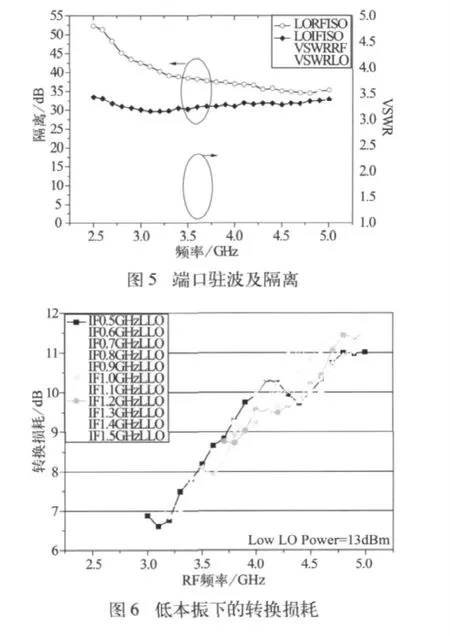
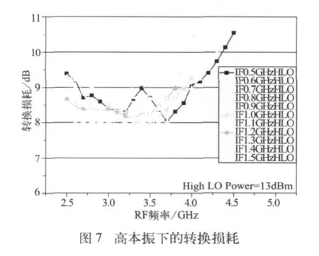
芯片實測結果如圖5、6、7所示,LO到IF和RF的隔離度分別為30dB和35dB,LO和RF端口駐波分別小于2和3.5。在低本振和高本振下,轉換損耗分別為11.5dB和10.5dB。
4 結果分析
實測結果與仿真比較吻合,同時轉換損耗的偏差也隨頻率上升而增大,這可能是由于折彎間距不夠而使得微帶線的內部耦合隨頻率加強,因此應加大此間距以改良整體性能。
[1]N. Marchand. Transmission-line conversion transformers[J].Electronics, 1994,17(12)∶142-145.
[2]K. S. Ang, I. D. Robertson. Analysis and Design of Impedance-Transforming Planar Marchand Baluns[J]. IEEE Transactions on Microwave Theory and Techniques, 2001,49(2)∶402-406.
[3]A. M. Pavio, R. M. Halladay. A distributed double-balanced dual-gate FET mixer[J]. IEEE GaAs IC Symp. 1988.177.
[4]R. Mongia, I. Bahl, P. Bhartia. RF and Microwave Coupled-Line Circuits[M]. Artech House Microwave Library, 1999.439.
[5]I. Robertson, S. Lucyszyn. RFIC and MMIC Design and Technology[M]. THE IEE, 2001. 220-230.
[6]H. K. Chiou, Y. R. Juang, H. H. Lin. Miniature MMIC star double balanced mixer using lumped dual balun[J]. ELECTRONICS LETTERS, 1997, 33(6)∶503-505.
[7]K. S. Ang, S. B. Economides, S. Nam,et al.. A compact MMIC balun using spiral transformers[M]. Proceedings of Asia Pacific Microwave Conference, Singapore, 1999.655-658.
A GaAs Monolithic Diode Double-balanced Mixer
CHEN Kun2, PENG Long-xin1,2, LI Jian-ping2
(1.National Key Laboratory of Monolithic Integrated Circuit and Modules,Nanjing210016,China;2.Nanjing Electronic Devices Institution,Nanjing210016,China)
A ring form double-balanced mixer (DBM) is designed by using 0.25μm GaAs process. Based on the characteristic of ring-diode DBM, the difference between RF balun and LO balun is proposed and then the two baluns are constructed by using Marchand balun and triformer balun respectively. The whole circuit is formed and optimized after the optimization of the two baluns over the bandwith. Finally the layout is made and simulated by EM tools. Some adjustment is executed on the layout to improve the performances. The measured conversion losses are about 11.5dB and 10.5dB under low and high LO frequency respectively with the LO power=13dbm. The isolation of LO port to IF port and LO port to RF port are better than 30dB and 35dB. The VSWR at LO port and RF port are less than 2 and 3.5. It shows that the measured results agree with the simulations pretty well.
double-balanced mixer (DBM); ring-diode; balun; MMIC; conversion loss
TN773.2
A
1681-1070(2010)09-0031-03
2010-06-13

陳 坤(1980-),男,安徽安慶人,畢業于華中科技大學電子科學與技術系,現為南京電子器件研究所碩士研究生,研究方向為微波單片集成電路設計。