Degradation and breakdown behaviors of SGTs under repetitive unclamped inductive switching avalanche stress
2022-09-24 08:01:30ChenkaiZhu朱晨凱LinnaZhao趙琳娜ZhuoYang楊卓andXiaofengGu顧曉峰
Chinese Physics B 2022年9期
Chenkai Zhu(朱晨凱) Linna Zhao(趙琳娜) Zhuo Yang(楊卓) and Xiaofeng Gu(顧曉峰)
1Engineering Research Center of IoT Technology Applications(Ministry of Education),Department of Electronic Engineering,Jiangnan University,Wuxi 214122,China
2Wuxi NCE Power Company,Ltd.,Wuxi 214028,China
Keywords: shield gate trench MOSFET, repetitive unclamped inductive switching stress, degradation, static and dynamic parameters
1. Introduction
Benefitting from high current handle capability and low Miller capacitance (CGD), shield gate trench (SGT) MOSFETs have shown great potential in automotive and industrial applications.[1,2]Unfortunately, when incorporated in power systems, the SGT MOSFETs suffer from unclamped inductive switching (UIS) stress, owing to the parasitic inductance or inductive load. This avalanche shock may lead to electrical degradation or severe failure to the Si-based power devices. So far,several constructive mechanisms have been proposed to explain the UIS degradation and failure behaviors.Kim and Nget al.suggested that the degradation could be attributed to triggering the parasitic bipolar junction transistor(BJT).[3,4]Pawelet al. performed experiment and simulation,revealing that the inhomogeneous switching phenomenon may lead to degradation of avalanche current.[5]Chenet al.suggested that suppressing the channel conduction could improve UIS ruggedness.[6]Tianet al. investigated on failure mechanism caused by non-uniform potential distribution of the shield gate.[7]However, previous researches mainly focus on the single-pulse avalanche shock. In order to verify the long-term reliability of SGT MOSFETs, an in-depth investigation on the repetitive UIS avalanche degradation and breakdown behaviors is necessary, which could contribute to the improvement of UIS ruggedness.
In this work, the degradation of conventional SGT (CSGT) MOSFETs and P-ring SGT (P-SGT) MOSFETs under repetitive avalanche stress is investigated. The static and dynamic parameters of the devices including drain leakage current (IDSS), breakdown voltage (BV), threshold voltage (Vth),output capacitance (COSS) and reverse transfer capacitance(CRSS) are monitored until breakdown. The degradation and failure mechanisms of the devices are discussed with the help of technology computer-aided design(TCAD)simulations and device failure photographs.
2. Device structure and experimental details
Figure 1 shows the cross-section views of the C-SGT and P-SGT fabricated by 0.5 μm PowerMOS manufacturing process in this work.

Fig.1. Cross-section views of(a)C-SGT and(b)P-SGT.
The key process flow of P-SGT is shown in Fig.2.Firstly,the N-epi layer is grown on Si substrate.Then,the trench etching,boron ion implantation,thermal oxidation and polysilicon deposition are performed respectively. Next, the polysilicon is etched back to form the shield gate,followed by etching of oxide. After the formation of thin gate oxide, a polysilicon layer is deposited into the gate trenches and etched back to form the gate electrode. Finally,the formation of the P-body,N+source region and the contacts can be realized by utilizing standard steps of a conventional trench MOSFET. Compared with C-SGT, an extra P-ring region is obtained by the boron ion implantation after trench etching. The introduction of Pring decreases the electric field(EF)crowding taking place at the bottom of trench,resulting in the increase ofBV.The main parameters of C-SGT and P-SGT are listed in Table 1.
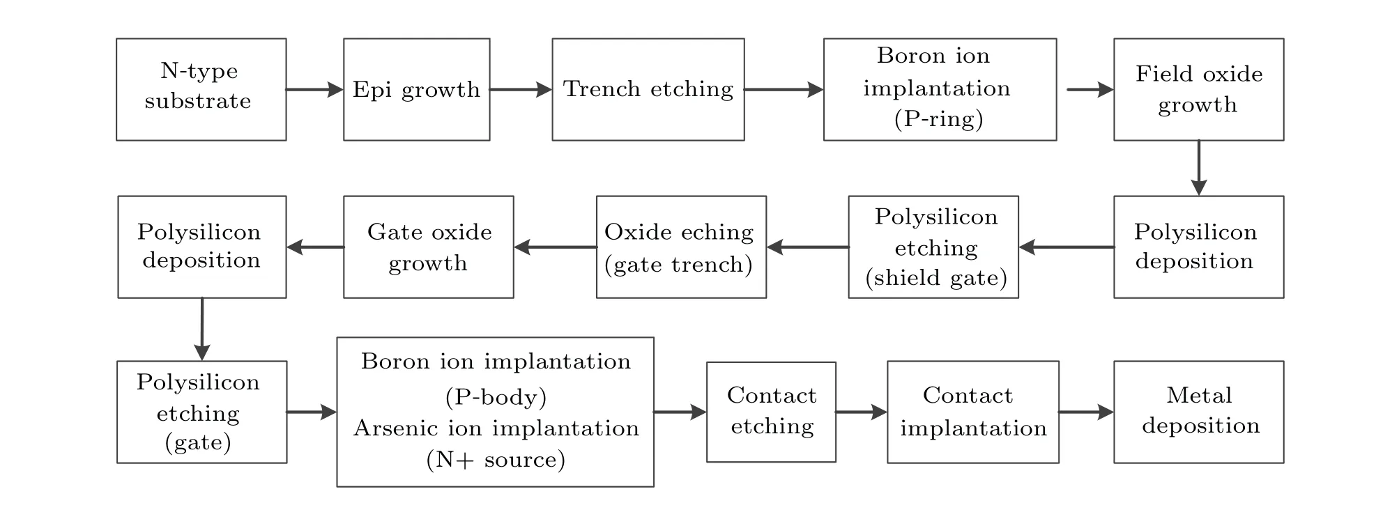
Fig.2. The key process flow of P-SGT.
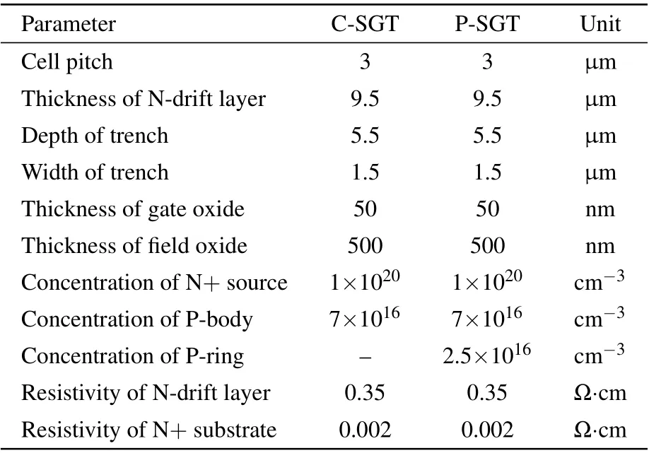
Table 1. Main parameters of C-SGT and P-SGT.
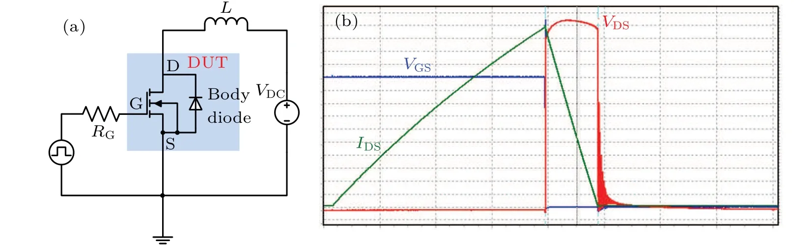
Fig.3. (a)Schematic of UIS test equivalent circuit and(b)the schematic diagram of VGS,VDS,and IDS versus time of single-pulse UIS test.
The schematic of UIS test equivalent circuit is shown in Fig. 3. In the circuit, a 10 V pulse generator is adopted to switch the device under test (DUT) between ON-state and OFF-state, accompanied with a 25 Ω gate resistor. Meanwhile,a direct current(DC)voltage source of 50 V for C-SGT and 60 V for P-SGT is applied, according to theBVlevel of the DUT.A 0.5 mH inductance is used as an inductive load,which stores energy when the DUT turns on, and discharges the avalanche current through the device from drain to source when the DUT turns off. Figure 3(b) shows the schematic diagram of gate-source voltage (VGS), drain-source voltage(VDS), and drain-source current (IDS) versus time of singlepulse UIS test. According to the equation
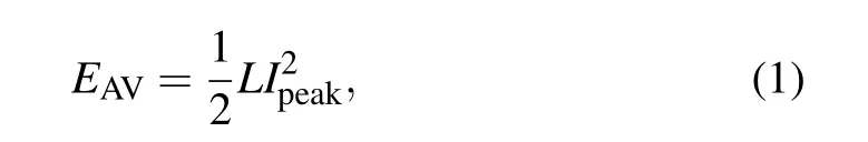
the avalanche energy(EAV)is 1.056 J for C-SGT and 1.156 J for P-SGT,respectively.To avoid the instantaneous failure,the selectedEAVis less than the single-pulse avalanche breakdown energy. Moreover,since Joule heating is the main cause of device breakdown,[8]a small air cooling equipment and copper heat sink are used to dissipate heat and decrease the influence of thermal accumulation.[9]
3. Results and discussion
Firstly,the impact of repetitive UIS stress on static parameters of DUTs are analyzed. In order to clarify the discharge path of UIS avalanche current,the mixed-mode simulation under the same UIS experiment condition is carried out by Sentaurus TCAD tools. Apart from some essential models (e.g.,doping dependency, high field velocity saturation, Shockley-Read-Hall recombination and Auger recombination),bandgap narrowing and UNIBO avalanche model are considered.[10]Figure 4 shows the simulated avalanche current flow path and impact ionization (I.I.) distribution of C-SGT and P-SGT. It can be seen that the body diode and conductive channel are the discharge paths of avalanche current for both devices.
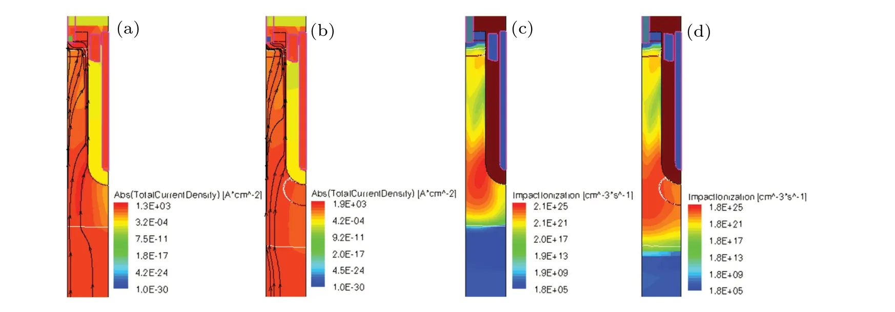
Fig.4. Simulated avalanche current flow path of(a)C-SGT and(b)P-SGT and impact ionization distribution of(c)C-SGT and(d)P-SGT.
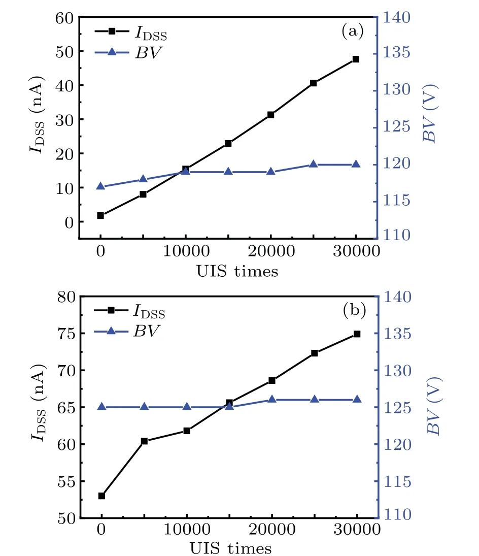
Fig. 5. Variation of IDSS and BV for (a) CSGT and (b) P-SGT under repetitive UIS tests.
For the purpose of investigating the degradation of body diode and gate oxide,the static parameters includingIDSS,BVandVthare monitored after every 5-k UIS tests until breakdown. In addition, theIDSSis measured atVGS=0 V andVDS=BV,theVthis tested atVGS=VDSandIDS=250μA by Keysight B1506A at room temperature. As shown in Fig. 5,theIDSSof C-SGT and P-SGT increase by 45.8 nA (2604%)and 21.9 nA(41.3%)from initial values after 30-k UIS tests,respectively. Meanwhile, theBVgradually increases before device breakdown as the number of UIS tests increases. Figure 6 depicts the variation ofVthfor C-SGT and P-SGT under repetitive UIS tests. The measured results exhibit a slight decrease inVthof C-SGT, but almost no degradation in that of P-SGT.
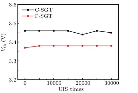
Fig.6. Variation of Vth for C-SGT and P-SGT under repetitive UIS tests.
Combining above experimental and simulation results,theIDSSdegradation for both devices can be explained as following: due to the high I.I. along the gate oxide (shown in Fig. 4), the generated hot holes trapped into the Si/SiO2interface. To verify the influences of these trapped holes, the interface-trapped charges with uniform distribution are placed along the Si/SiO2interface of the devices in TCAD simulations. Figures 7(a),7(b)and 7(d),7(e)show the 2-D EF distribution in the fresh device and stressed device of C-SGT(with hole concentration of 7.9×1011cm-2)and P-SGT(with hole concentration of 7.1×1011cm-2)atVDS=100 V,respectively.The hole concentration is estimated according to theIDSSof the 30000thUIS test. Figures 7(c) and 7(f) show the vertical EF curves along AA'and BB'cutline,respectively. As can be seen, compared with the fresh device, the holes injected into the gate oxide widen the boundary of depletion layer toward the surface of stressed device for both devices. Correspondingly,the EF at the P-body/N-drift junction is enhanced,leading to an increase ofIDSS.
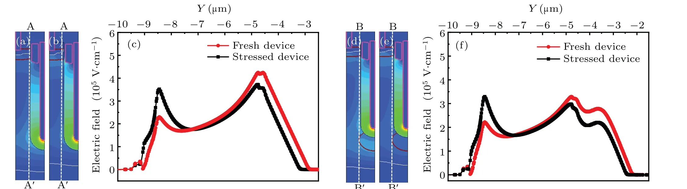
Fig.7. The 2D EF distribution in the(a)fresh device and(b)stressed device of C-SGT,(c)vertical EF curves along AA',and EF distribution in the(d)fresh device and(e)stressed device of P-SGT,(f)vertical EF curves along BB'.
Besides,it worth noting that theBVof both devices shows an increasing trend before breakdown(shown in Fig.5). In order to explain this interesting phenomenon, the degradation process under repetitive UIS tests is simulated by increasing the trapped hole concentration of both devices.In Fig.8,as the trapped holes concentration increases,theBVof both devices rise initially and then start to drop rapidly when the trapped holes concentration exceeds 8.3×1011cm-2.[11]It implies that if the number of UIS tests exceeds a certain value, the DUTs are facing extreme high EF at the gate oxide,a rapid increase of trapped hole concentration and instantaneous breakdown,which is in good agreement of preceding experiment results.
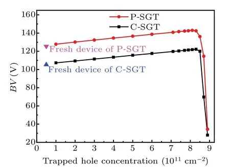
Fig.8. The BV of C-SGT and P-SGT with different trapped hole concentration.
To prove the mechanism of the holes trapping,theBVof C-SGT and P-SGT are monitored under the ambient temperature of 450 K after the repetitive avalanche. As shown in Fig. 9, theBVof both devices recover with the time increasing,because of the detrapping of holes from the SiO2dielectric layer under high temperature.[11]
Further, considering the switching applications of power devices, the degradation of dynamic characteristics for CSGT and P-SGT are investigated. In SGT MOSFETs, the shield gate is introduced to alleviate the EF non-uniformity in N-type epitaxial layer and reduce gate-to-drain capacitance(CGD). However, the output capacitance (COSS) is several times greater than the single-gate trench MOSFET,causing a reduction in the switching frequency.[12]Therefore, we focus on the dynamic parameter ofCOSSin this work.

Fig.9. The BV variations of(a)C-SGT and(b)P-SGT under the ambient temperature of 450 K after the repetitive avalanche.
Figure 10 shows theCOSSandCRSSof C-SGT and PSGT after every 10-k UIS tests until breakdown. In theCVmeasurement, the frequency used is 1 MHz. As shown in Fig.10(a),theCOSSof C-SGT significantly increases when the drain voltage is in the range of 35 V to 60 V, while theCRSSshows no degradation.Since theCOSSis composed of the gatedrain capacitance(CGD,also calledCRSS)and the drain-source capacitance (CDS), the variation ofCOSSis mainly caused by the increase ofCDS. The increase ofCDSis owing to the reduction of depletion layer of P-body/N-drift junction (shown in Fig. 7), caused by the hot holes injected into the field oxide during repetitive UIS stress. In P-SGT,theCOSSandCRSSalmost remain unchanged, benefitting from the decreasing of the impact ionization rate at bottom of field oxide caused by the existence of P-ring.[13]
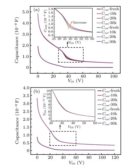
Fig. 10. The COSS and CRSS of (a) C-SGT and (b) P-SGT measured after every 10-k UIS tests.
After repetitive avalanche breakdown,the de-capsulation of DUTs are carried out. The source metal on the surface of the DUTs are removed using hydrochloric acid. Figure 11 shows the failure photographs of C-SGT and P-SGT, respectively. In both devices, the failure points are located in the cell region instead of the termination region, illustrating that the termination plays an important protective role in repetitive UIS avalanche stress. Based on the above analysis, two reasons may account for repetitive avalanche breakdown. Firstly,the high I.I.arouses a raised electron-hole combination in the P-body/N-drift junction. Since the energy released by combination is absorbed by the crystal lattice of silicon material, it leads to an increase of lattice temperature. When the temperature approaches the intrinsic temperature,the device thermal breakdown. Secondly,the injection of holes into the gate oxide layer increases the EF near the gate oxide. When the EF near the gate oxide exceeds the EF near the field oxide, the device breakdown.
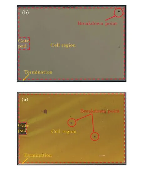
Fig.11. The failure photographs of(a)C-SGT and(b)P-SGT.
4. Conclusion and perspectives
The degradation and breakdown behaviors of C-SGT and P-SGT under repetitive avalanche stress is investigated in detail.As the hot holes are continuously injected into the Si/SiO2interface and the lattice temperature increases, both devices feather different degrees of degradation on static and dynamic parameters. Furthermore, compared with C-SGT, the P-SGT suffer from limited damage of body diode and oxide layer,benefitting from the grounded shield gate and floating P-ring.In term of the long-term reliability of SGT-MOSFETs in practical applications,the degradation ofIDSS,BVandCOSSshould be carefully considered.
Acknowledgements
Project supported by the National Natural Science Foundation of China(Grant No.61504049),Jiangsu Province Postdoctoral Science Foundation (Grant No. 2018K057B), and the Fundamental Research Funds for the Central Universities,China(Grant No.JUSRP51510).
- Chinese Physics B的其它文章
- Erratum to“Accurate determination of film thickness by low-angle x-ray reflection”
- Anionic redox reaction mechanism in Na-ion batteries
- X-ray phase-sensitive microscope imaging with a grating interferometer: Theory and simulation
- Regulation of the intermittent release of giant unilamellar vesicles under osmotic pressure
- Bioinspired tactile perception platform with information encryption function
- Quantum oscillations in a hexagonal boron nitride-supported single crystalline InSb nanosheet