
Effects of electrical stress on the characteristics and defect behaviors in GaN-based near-ultraviolet light emitting diodes
2022-06-29 09:23:50YingZheWang王穎哲MaoSenWang王茂森NingHua化寧KaiChen陳凱ZhiMinHe何志敏XueFengZheng鄭雪峰PeiXianLi李培咸XiaoHuaMa馬曉華LiXinGuo郭立新andYueHao郝躍
Chinese Physics B 2022年6期
Ying-Zhe Wang(王穎哲) Mao-Sen Wang(王茂森) Ning Hua(化寧) Kai Chen(陳凱)Zhi-Min He(何志敏) Xue-Feng Zheng(鄭雪峰) Pei-Xian Li(李培咸) Xiao-Hua Ma(馬曉華)Li-Xin Guo(郭立新) and Yue Hao(郝躍)
1Key Laboratory of Wide Bandgap Semiconductor Materials and Devices,School of Microelectronics,Xidian University,Xi’an 710071,China
2Shanghai Aerospace Electronic Technology Institute,Shanghai 201109,China
3School of Advanced Materials and Nanotechnology,Xidian University,Xi’an 710071,China
4School of Physics and Optoelectronic Engineering,Xidian University,Xi’an 710071,China
Keywords: light emitting diodes,GaN,electrical stress,defect
1. Introduction
GaN-based near-ultraviolet (NUV, 320–400 nm) light emitting diodes (LEDs) have received extensive attention in practical applications such as curing,short-distance fiber communications, biosensors, and materials processing.[1–4]Due to the advantages of small dimensions, low power consumption, and environmental protection, the market for NUV LEDs is continuously expanding. However, during operation, some reliability problems, such as optical power (OP)decay,have been the bottleneck for the further development of devices.[5–7]Therefore,it is essential to study the degradation mechanisms of GaN-based NUV LEDs under electrical stress.
For GaN-based LEDs, it is suggested that electrical stress-induced degradation can be attributed to the generation or the propagation of point defects activated by carrier transport, such as vacancies or anti-site defects.[8–12]In addition,effects of dislocations on device degradation cannot be ignored for NUV LEDs[13–15]due to the lack of In-rich clusters that separate carriers from dislocations.[16]However,the behavior of defects that cause device degradation has yet to be confirmed. The process of defect generation/propagation under electrical stress should be further demonstrated.
In this work,we investigate the degradation mechanisms of NUV LEDs under electrical stress from the aspect of defects. Under different stress time, the optical and electrical characteristics in NUV LEDs are evaluated by electroluminescence (EL) and current–voltage (I–V) measurement. Meanwhile,the deep level transient spectroscopy(DLTS)measurement is applied to characterize the defect behavior, including defect concentration,energy level,and cross section.From the DLTS results under different filling pulse widths, the defect spatial distribution is analyzed in detail. In addition,photoluminescence (PL) measurement is also introduced to assist in judging the origin of the defect leading to degradation.
2. Device and experiments
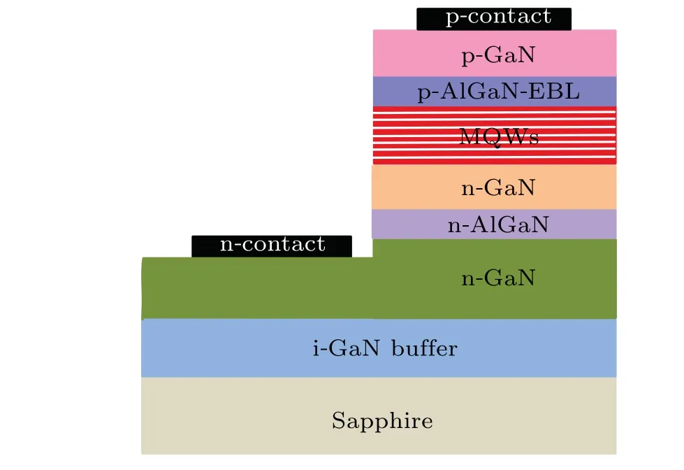
The experimental analysis was performed simultaneously on five NUV LEDs with a peak emission wavelength of 385 nm from the same wafer.As shown in Fig.1,from bottom to top, the structure consists of a sapphire substrate, an undoped GaN buffer layer,a 900-nm-thick Si-doped n-type GaN layer, a 30-nm-thick n-Al0.05Ga0.95N layer, a 400-nm-thick lightly Si-doped GaN layer, an active region, a 30-nm-thick Mg-doped p-Al0.15Ga0.85N electron blocking layer(EBL),and a 240-nm-thick p-GaN layer. The active region consists of eight-period Si-doped multiple quantum wells (MQWs) using 10-nm-thick GaN barriers and 1-nm-thick In0.07Ga0.93N wells. The chip size is 1143 μm×1143 μm. NUV LEDs were stressed with a constant current of 600 mA,which was twice the nominal operation current (300 mA) and can cause great degradation. In order to be closer to the actual application,the electrical stress was applied under room temperature without any heat dissipation. After electrical stress, the device characteristics and defect behaviors were characterized when the junction temperature returned to room temperature.
3. Results and discussion
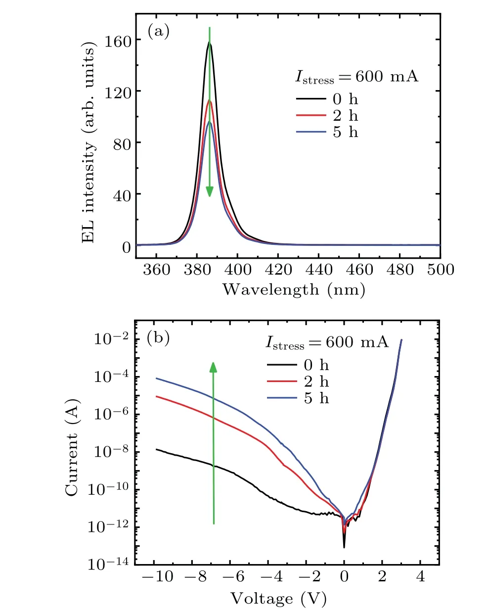
The kinetics of the optical power decrease in NUV LEDs were investigated during electrical stress using electroluminescence (EL) measurement. As shown in Fig. 2(a), the optical power decreases evidently with the increasing stress time. In GaN-based photoelectric devices, it can be attributed to the increase of non-radiative recombination centers.[17]The electrical characteristics were also characterized usingI–Vmeasurement at room temperature from-10 V to 3 V.It is shown in Fig. 2(b) that the reverse leakage current (Ir) increases by several orders of magnitude after stress. Previous studies demonstrated thatIris associated with the parasitic leakage path.[18]In addition, the current under low forward bias also increases after stress,which can be ascribed to the increase of trap-assisted tunneling (TAT) current.[19]Both non-radiative recombination centers,parasitic leakage paths,and TAT mechanisms are all tightly correlated with defects within or around the active region.[20,21]Therefore,the variation of the defects in NUV LEDs during electrical stress should be pressingly studied.
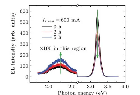
Firstly, photoluminescence (PL) measurement was carried out using a He–Cd laser emitting at 325 nm at room temperature to detect and identify the defects in NUV LEDs macroscopically. Different from EL measurement,the results in PL measurement are not related to injection efficiency,making it possible to characterize the defect luminescence characteristics more intuitively.[22]As shown in Fig. 3, the appearance of the band-to-band peak at 3.2 eV indicates that the region detected in PL measurement includes the active region.With the increasing stress time, a yellow luminescence (YL)band centered around 2.2–2.3 eV increases,indicating that the concentration of some defects increases under the stimulation of electrical stress. In the GaN material system, many previous studies demonstrated that the YL band could be attributed to Ga vacancy(VGa)related defects.[23,24]However,the origin of the defects should be further confirmed, and the evolution mechanism of the defects should be studied deeply.
DLTS measurement,which can quantitatively extract the defect physical parameters,[25]has been applied to investigate the defect behaviors deeply.Figure 4(a)shows the DLTS spectra scanned from 490 K to 60 K with a quiescent bias of-7 V,a filling pulse bias of 2 V,and a filling pulse width of 10 ms.These bias and temperature values were chosen to explore the defects in the n-type active region comprehensively. In our measurement system, the positive and negative peaks are associated with majority-carriers (electron) traps and minoritycarriers (hole) traps, respectively. With the increase of stress time,a positive peak A at~70 K almost has no change. Such a narrow peak at low temperature may not be associated with the defects but with the emission from QW to the conduction band.[26]The activation energy of peak e1 is 0.08 eV,which may be related to the conduction band offset of the In-GaN/GaN quantum well.[27]The slight decrease of peak e1 after stress can reflect the decline of QW quality.
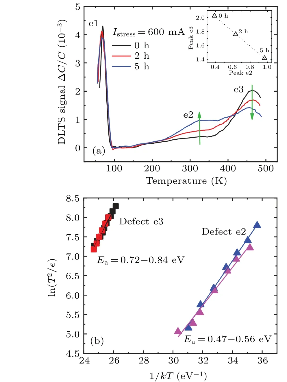
In this work,more attention should be paid to peaks corresponding to defects in the DLTS spectrum(Fig.4(a)).Under the stimulation of electrical stress,a positive peak e2 at~310 K increases. The activation energy and cross section of defect e2 are extracted from the Arrhenius plot in Fig.4(b),which are 0.47–0.56 eV and 3.2×10⁻¹⁷–2.7×10⁻¹⁶cm2, respectively.In addition,compared with the PL results,the increased peak e2 may correspond to the increased YL peak in the PL spectrum. Combing the YL-related feature with the activation energy,defect e2 can be attributed to VGarelated complex,possibly involving oxygen, e.g., VGa–ON.[10,28,29]Interestingly,during increasing of concentration of defect e2,the concentration of intrinsic defect e3(a positive peak at~460 K)with the activation energy 0.72–0.84 eV and cross section 1.8×10⁻¹⁷–9.8×10⁻¹⁶cm2decreases. The linear relationship in the inset of Fig.4(a)suggests a direct correlation between the defects e2 and e3. In other words,the increase of concentration of defect e2 after stress may result from the decreasing concentration of defect e3.
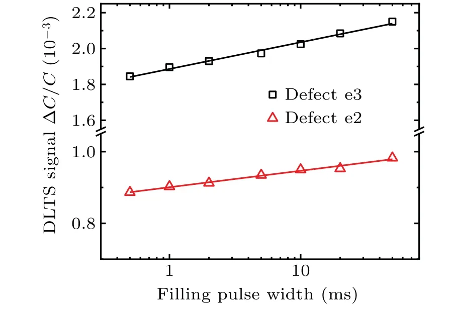
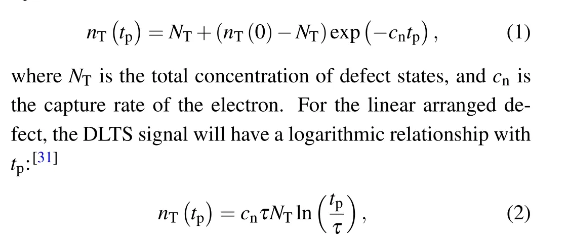
Moreover,in the GaN system,besides the non-interacting point defects, linearly arranged defects such as point defects along dislocations also need to be focused on. The noninteracting and linear arranged point defects will exhibit completely different behaviors. It is difficult to identify defects accurately merely through the activation energy. Therefore,it is significant to analyze the defect spatial configuration using DLTS measurement under different filling pulse widths.[30]For the non-interacting point defects, the concentration of occupied defect states (nT) corresponding to the DLTS signal will be exponentially correlated to the filling pulse width(tp):[31]
whereτis the characteristic time. As shown in Fig. 5, both the DLTS signals of defects e2 and e3 are logarithmically correlated to the filling pulse width, indicating that these two defects are point defects along dislocations. The evolution of defects develops around dislocations, possibly due to the relatively concentrated current flow path.[32,33]The characteristic of the electron trap and its contribution to the yellow band peak further demonstrate that defect e2 is likely related to VGaand oxygen related complex(e.g.,VGa–ON)along dislocation.[34–36]This defect may act as the non-radiative recombination center and parasitic leakage path and then degrade NUV LEDs.
So far, there is still a question about the origin of the intrinsic defect e3 and the evolution process between these two defects. For the defect e3 with the activation energy of 0.72–0.84 eV, there are some possible origins such as VGa–ON–H,[37]VN–H,[38]VGa–VN.[23]Among them, the formation energies of VN–H and VGa–VNare very high in the n-type region,[23,39]which leads to the little possibility of formation during growth. It is more likely to attribute the intrinsic defect e3 to VGa–ON–H, mainly for three reasons. Firstly, it is now well accepted that oxygen and hydrogen can often be the background contaminants during growth,[40]and VGais likely to form a complex with impurities like O and H during growth due to the low formation energy.[24,41]Secondly,the defect luminescence will decrease when the defects are passivated with H.[42]This phenomenon corresponds to the low YL peak in the PL spectrum of the fresh device. The YL intensity in the fresh device is nonzero because not all defects were passivated by H during growth. Thirdly,the dehydrogenation process has been observed in other nitride-based devices, and electrical stress will enhance this process.[43–45]Under high injection current,the junction temperature rises evidently,resulting in sufficient energy for carriers to transfer to the lattice, and the dehydrogenation process is prone to occur.[45,46]Therefore, the dehydrogenation of the previously passivated VGaand oxygen related complex defects after stress is likely to result in the activation of the VGarelated defects(e.g.,VGa–ON)and then induce the device degradation.
4. Conclusions
In summary,we have investigated the degradation mechanism of GaN-based NUV LEDs under electrical stress from the defect point of view. The optical power decreases,and the leakage current increases evidently after stress, which results from the increase in the concentration of defects with the energy level of 0.47–0.56 eV accompanied by the decrease of defects with the energy level of 0.72–0.84 eV.Combining the activation energy,the logarithmic relationship between DLTS signal and filling pulse width,with the increase of YL peak in PL spectrum during stress,the defects with increasing concentration can be attributed to VGaand oxygen related complex along dislocation. This defect may act as the non-radiative recombination center and parasitic leakage path, leading to device degradation.The defects with decreased concentration after stress can be ascribed to VGarelated defects that were passivated by H inherent during growth. During electrical stress,the dehydrogenation process around dislocations is likely to be the main origin for the degradation of GaN-based NUV LEDs.Therefore,more attention should be paid to the dislocation and the unintentionally induced hydrogen during growth in NUV LEDs.
Acknowledgements
Project supported by the National Natural Science Foundation of China(Grant Nos.62104180,61974115,11690042,61634005,61974111,12035019,and 61904142),and the Fundamental Research Funds for the Central Universities (Grant No.XJS221106),and the Key Research and Development Program of Shaanxi,China(Grant No.2020ZDLGY03-05).
- Chinese Physics B的其它文章
- Switchable terahertz polarization converter based on VO2 metamaterial
- Data-driven parity-time-symmetric vector rogue wave solutions of multi-component nonlinear Schr¨odinger equation
- Neutron activation cross section data library
- Multi-phase field simulation of competitive grain growth for directional solidification
- A novel similarity measure for mining missing links in long-path networks
- Dynamically controlled asymmetric transmission of linearly polarized waves in VO2-integrated Dirac semimetal metamaterials