
Tunable electronic properties of GaS-SnS2 heterostructure by strain and electric field
2022-04-12 03:44:46DaHuaRen任達(dá)華QiangLi李強(qiáng)KaiQian錢楷andXingYiTan譚興毅
Chinese Physics B 2022年4期
Da-Hua Ren(任達(dá)華) Qiang Li(李強(qiáng)) Kai Qian(錢楷) and Xing-Yi Tan(譚興毅)
1School of Information Engineering,Hubei Minzu University,Enshi 44500,China
2Science of Physics and Technology,Wuhan University,Wuhan 430072,China
3School of Advanced Materials and Mechatronic Engineering,Hubei Minzu University,Enshi 44500,China
4Department of Physics,Chongqing Three Gorges University,Wanzhou 404100,China
Keywords: GaS-SnS2 heterostructure,type-II band alignment,optical properties,density functional theory
1. Introduction
Van der Waals (vdW) heterostructures can be used in unusual electronic devices because of their peculiar physical properties and excellent performances.[1]Additionally,vertically stacked heterostructures have innovative applications in electronic devices,such as ultrathin photodetectors,[2]solar cells,[3]memory devices,[4]flexible sensors, and transistors.[5,6]Specifically, two-dimensional (2D) vdW heterostructure with type-II band alignment has promising potentials in photovoltaics devices and photocatalysts[7-11]due to their fascinating electronic and optical properties. In type-II heterostructures, the photogenerated holes and electrons are spatially located in different layers. As a result, the recombination of carriers can be effectively prevented and the light energy utilization is significantly enhanced.[12]Moreover, GaS is a typical layered group III-VI compound and each layer is composed of S-Ga-Ga-S repeating units along thecaxis withD3hsymmetry. The interlayer interactions between layers belong in weak vdW force. The GaS can be used for a promising near-blue light emitting devices because of the indirect band gap of 2.5 eV.[13]More interestingly, monolayer GaS can be easily mechanically cleavaged.[14]The photodetectors based on GaS nanosheet have higher photoresponsivity than graphene, 2D MoS2.[15]Recent researches indicate that the vdW heterostructures based on monolayer GaS are able to exhibit type-II band alignment, such as GaS-GaSe,[16]GaSMoSe2,[17]and GaS-InS.[18]
Furthermore,tin disulfide(SnS2)has attracted intense attention in solar energy conversion, optoelectronics, and photocatalyst because of its CdI2-type layered structure with a sustainable band gap (2.2 eV-2.35 eV) and high electrical conductivity.[19]The SnS2consists of an S-Sn-S triple layer and the interlayer interaction belongs in the vdW force. The SnS2single-layer is synthesized by liquid exfoliation. The experimental researches indicate that the SnS2single-layer is of a semiconductor with a band gap of 2.29 eV and can be used in visible-light water splitting due to the high photo-conversion efficiency.[20]However,an inconvenient band edge alignment of pristine SnS2hinders the efficient photocatalyst from splitting water.[21]Recent efforts have demonstrated that the electronic and optical properties of SnS2can be greatly tailored by external means, such as doping,[22]electric field,[23]and stacking heterostructure with other 2D materials.[24]
Up to now,the combination of SnS2with different semiconductors, such as SnS2-TiO2,[24]SnS2-g-C3N4,[25]SnS2-SnO2,[26]SnS2-RGO,[27]and ZrS2-SnS2,[28]has been reported to enhance photocatalytic performance. In addition,the heterostructure based on 2D SnS2,such as SnS2-BiPO4[29]heterostructure,are able to be formed into a type-II band structure, which shows good electronic and optical behaviors in photocatalyst and optoelectronic applications. Even though there exist a few of researches on 2D heterostructure based on 2D SnS2,the understanding of the role and evolution of SnS2in the GaS-SnS2heterostrucutre has not been demonstrated.
Herein,we constructe a novel 2D GaS-SnS2heterostructure and study the structural, electronic, optical, photocalytic properties. Note that 2D SnS2, together with 2D GaS, can form a vdW heterostructure due to their similar structures and same lattice constants. Generally,it is also worth studying the superior structure and excellent properties of GaS-SnS2heterostructure, which could potentially provide a platform for applications in photocalyst and optoelectronic devices.
2. Computational methods
Ab initio calculations were performed within the framework of density functional theory (DFT).[30,31]as implemented in the Viennaab initiosimulations package(VASP).[32]Electronic exchange and correlation effects were described with the Perdew-Burke-Ernzerhof (PBE)[33]functional of generalized gradient approximation (GGA)[34]and HSE06[35]hybrid function. Electron-ion interactions were treated with the projector augmented wave (PAW)method,[36,37]with an energy cutoff being 500 eV and Brillouin zone sampling ofK-mesh set to be 11×11×1 for relaxation. TheK-mesh points for density of states (DOS)and energy band structure calculations were assumed to be 13×13×1, and the energy criterion was set to be 105eV until the residual force was smaller than 103eV/°A.Especially,the vacuum layer thickness is fixed at more than 25 °A to avoid spurious interactions in the neighboring images. As the longrange vdW interaction is important for holding the 2D heterostructure together, the vdW-D3 approach[38]was used to describe long-range electron correlation effects.
The optical properties of 2D GaS-SnS2heterostructures are described by the complex dielectric functionε(ω) =ε1(ω)+iε2(ω),whereε1(ω)andε2(ω)are the real part and the imaginary part,respectively. At the same time,the imaginary part is calculated by summing up all possible transitions from the occupied to the unoccupied states,which is related to the band structure in the absorption behaviors.[39]The imaginary part is given by
wherePis the principal value. The absorption coefficient is then obtained as follows:[40,41]
3. Results and discussion
3.1. Stability and structures
Stacking patterns can modulate the electronic properties of the vdW heterostructures. In stacking (AA), the Sn atom is placed on the top of Ga atom, while the S atom in SnS2layer is situated on the top of S atom in GaS layer. In stacking(AB),the S atom in SnS2layer is placed on the top of Ga atom while the Sn atom is located at the hexagonal site. In stacking (AC), the Sn atom is placed on the top of S atom in GaS layer, while the S atom in SnS2layer is settled at the hexagonal site. In stacking (AD), the Sn atom is placed on the top of S atom in GaS layer while the S atom in SnS2layer lies on the top of Ga atom. We check the structural stability of these heterostructures by calculating their binding energy values,interlayer distances and thermal stabilities. Therefore,a typical stacking configuration (AA) is constructed due to the lowest adhesion energy and thermal stability. The relaxed structure is shown in Fig.1. After relaxation,the equilibrium lattice constants of GaS monolayer(a=b=3.585 °A),SnS2monolayer(a=b=3.699 °A) and AA stacking GaS-SnS2heterostructure (a=b= 3.636 °A), calculated with GGA-PBE, are in consistence with other reported results.[14,16-19]It is clear that the hexagonal unit parameter of GaS-SnS2heterostructure is 3.636 °A.The lattice mismatch of GaS-SnS2heterostructure is 1.7%,meaning that the structure of GaS-SnS2heterostructure is acceptable.
To describe the vdW interaction,the interface binding energy(ΔE)of GaS-SnS2heterostructure is calculated to be

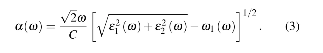
where ΔErefers to the interface binding energy at the interface of GaS-SnS2heterostructure;EHS,EGaS,ESnS2,Srepresent respectively the total energy of heterostructure, GaS monolayer, SnS2monolayer, the interface areas of the heterostructure. Obviously, the interface binding energy of GaS-SnS2heterostructure is-27.8 meV/°A2, demonstrating that the interaction between two layers is physically vdW force. The interface binding energy is negative,suggesting that the GaSSnS2heterostructure has favorable energy during the formation. In addition,the AIMD simulation of the GaS-SnS2heterostructure for the most favorable stacking AA pattern is also performed to confirm the thermal stability at room temperature as can be seen in Fig.2. Obviously,the variation of total energy of the GaS-SnS2heterostructure is quite small during 6800 fs,indicating that the GaS-SnS2heterostructure is thermally stable at room temperature.

Fig.1. Relaxed structures of four typical stacking patterns of GaS-SnS2 heterostructure,with red,yellow,and blue spheres representing Ga,S,and Sn atoms,respectively.
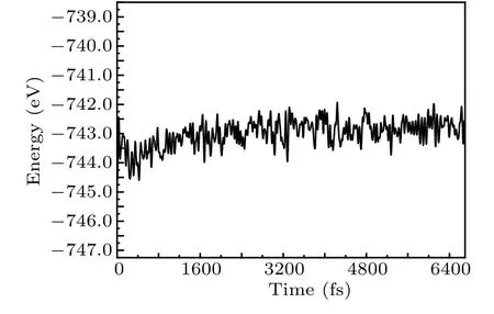
Fig.2. Thermal stability of GaS-SnS2 heterostructure.
As shown in Fig.3,the optimal distance between S atom in the GaS layer and S atom in the SnS2layer is 3.705 °A,meaning that no bonds between S atoms are formed and this heterostructure is formed by the same magnitude order of vdW forces as typical vdW graphite.[42]
Fig. 3. Plot for the 4-th order polynomial fit interface binding energy as a function of interlayer distance of GaS-SnS2 heterostructure.
3.2. Electronic properties
In the following, projection-resolved band structures of GaS monolayer, SnS2monolayer, GaS-SnS2heterostructure are depicted in Fig. 4. The GaS-SnS2heterostructure is an indirect band gap semiconductor. The valence band maximum (VBM) and the conduction band minimum (CBM) of the GaS-SnS2heterostructure are located at theMpoint andK →Gof Brillouin zone (BZ). The band gap of GaS-SnS2heterostructure is 1.82 eV from the HSE06 calculation,smaller than those of both individual GaS (3.19 eV) monolayer and individual SnS2(2.31 eV)monolayer,which accord well with the theoretical values of GaS(3.29 eV),[15]SnS2(2.39 eV).[43]Specially,GaS-SnS2heterostructure has a type-II band alignment, which is beneficial to separating the photogenerated holes and electrons in different layers, preventing the carriers from being recombined, and enhancing the light energy utilization. Therefore, the band gap of the GaS-SnS2heterostructure can be significantly changed by vertically stacking the heterostructure,which can provide a good opportunity to work on band engineering and photoelectronic device designs.
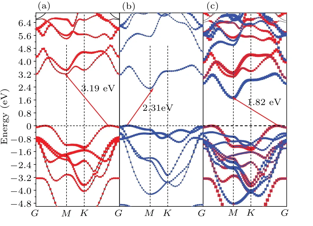
Fig. 4. Projection-resolved band structure of (a) GaS monolayer, (b) SnS2 monolyer,and(c)GaS-SnS2 heterostructure,with red and blue lines denoting contributions from GaS and SnS2 layers,respectively.
As reflected in the projection-resolved band structure,the band gap of GaS monolayer decreases due to the downshift of CBM atMpoint as well as the upshift of VBM atK →Gpoint. The contribution of VBM of GaS-SnS2heterostructure is GaS layer and that of CBM is SnS2layer,in which the red and blue lines present the DOS of GaS and SnS2layer in GaS-SnS2heterostructure,respectively,in Fig.5. Obviously,in the GaS-SnS2heterostructure, the VBM and CBM are respectively confined in GaS and SnS2layer,respectively,indicating that the GaS-SnS2heterostructure has a type-II band alignment.
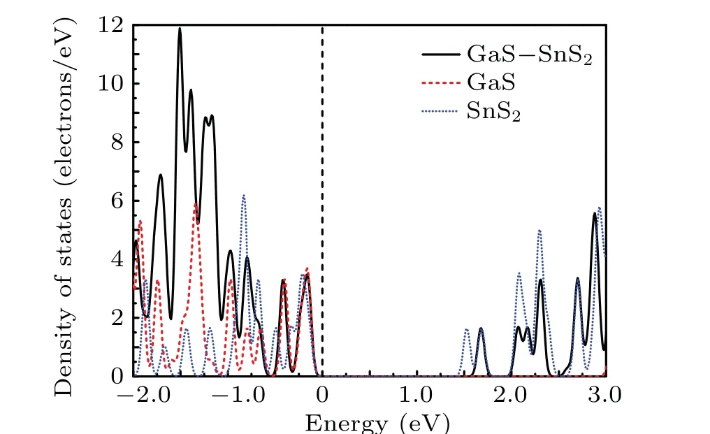
Fig.5. Projected density of states(PDOS)of GaS monolayer,SnS2 monolayer, GaS-SnS2 heterostructure, where Fermi level is set to zero as indicated by the black dashed line.
3.3. Effect of external electric field and biaxial strain on band gap of GaS-SnS222 heterostructure
External electric field is extensively considered as an efficient strategy to expand the semiconductors with desirable band gap into photoelectronic devices. Therefore, it is extremely important that an external electric field (Eext) be applied to changing the band gap of GaS-SnS2heterostructure as depicted in Fig.6. The band gap of GaS-SnS2heterostructure, which remains indirect semiconductor, changes a lot in theEextrange from-0.1 V/°A to 0.1 V/°A.Note that the electric field direction from the bottom (GaS layer) to the top (SnS2layer) is the positiveZdirection ofEext, perpendicular to the interface. The band gap decreases from-0.1 V/°A to 0.1 V/°A,which accelerates electrons(holes)from the conduction band-CB(valence band-VB)of the SnS2(GaS)layer to the CB(VB)of the GaS(SnS2)layer as shown in Fig.6(b).
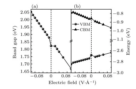
Fig.6. Variation of(a)band gap and(b)band alignment of GaS-SnS2 heterostructure with external electric field.
Biaxial strain is effectively able to tailor the electronic performance of heterostructure. Here, the effect of biaxial strain from-8% to 10% on the electronic property of GaSSnS2heterostructure is discussed, namely the corresponding lattice parameter of the heterostrucutre unit cell is effectively modified. Fortunately,the structure of the heterostructure under biaxial strain is successfully relaxed and has the hexagonal lattice symmetry according to the same state of the irreducible Brillouin zone. The change of the band gap under biaxial strain is shown in Fig. 7. As the compress strain increases from-4% to-8%, the band gap first decreases, for the VBM increases more rapidly than the CBM.And the compress strain increases from 0 to-4%, the band gap then increases due to the more fast-growing CBM. Meanwhile, the band gap decreases monotonically when the tensile strain increases from 0 to 10%due to the CBM moving more speedily down to fermi level than the VBM.
Although the outermost two S layers in the GaS-SnS2heterostructure have the same electronegativity, the sixth Sn layer on the SnS2side has greater electronegativity (2.44e)than the second Ga layer on the GaS side(2.14e). Therefore,the electrons at the interface are depleted on the GaS side but accumulated on the SnS2side,forming a built-in electric field from GaS layer to SnS2layer. The smaller charge transfer at the interface leads to the weaker interaction between Sn and Ga atoms.
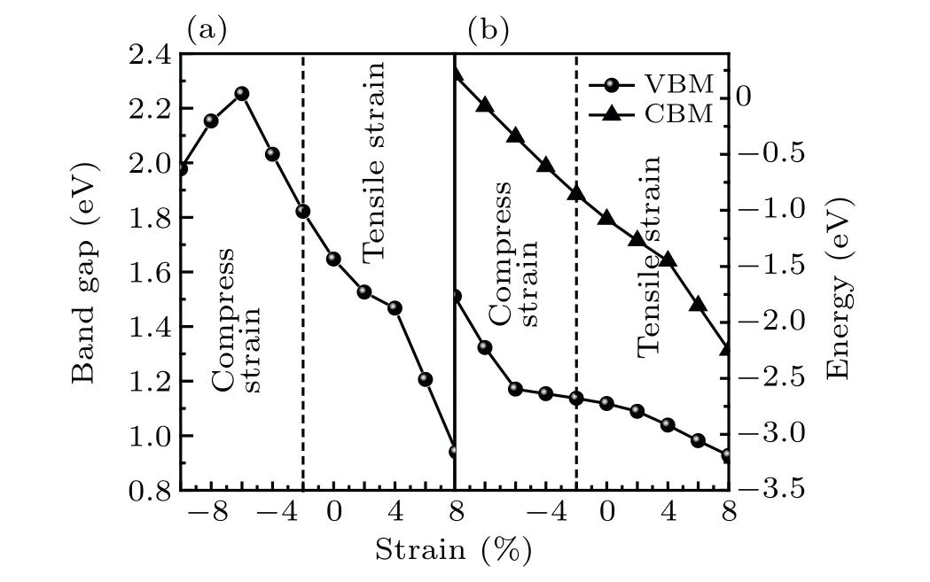
Fig.7. Variation of(a)band gap and(b)band alignment with biaxial strain of GaS-SnS2 heterostructure.
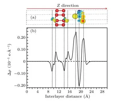
Fig.8. (a)Charge density difference and(b)planar-averaged charge density difference of GaS-SnS2 heterostructure along Z direction.
The planar-averaged charge density difference along theZdirection is described as Δρ=ρGaS-SnS2-ρGaS-ρSnS2,where,ρGaS-SnS2,ρGaS,ρSnS2are the planar-averaged charge densities of GaS-SnS2heterostructure, GaS monolayer, and SnS2monolayer. As shown in Fig. 8, the positive value and the negative value represent the charge accumulation and the charge depletion, respectively. Both electrons and holes under built-in electric field move towards the opposite directions,which can accelerate the separation of photo-generated electrons or holes to improve photocatalytic activity.
3.4. Photocatalyst and absorption behaviors
The absorption coefficient of GaS-SnS2heterostructure is calculated,and the results are shown in Fig.9(a). It is clear that the first peak in the absorption spectrum of GaS-SnS2heterostructure is locates at 2.25 eV,which is mainly contributed by the SnS2layer. The absorption behavior of GaS-SnS2heterostructure is more improved than that of the individual GaS monlayer and SnS2monolayer. The absorption spectrum of GaS-SnS2heterostructure covers the visible light, which makes it well suitable for the application of optoelectronic devices in visible light region.
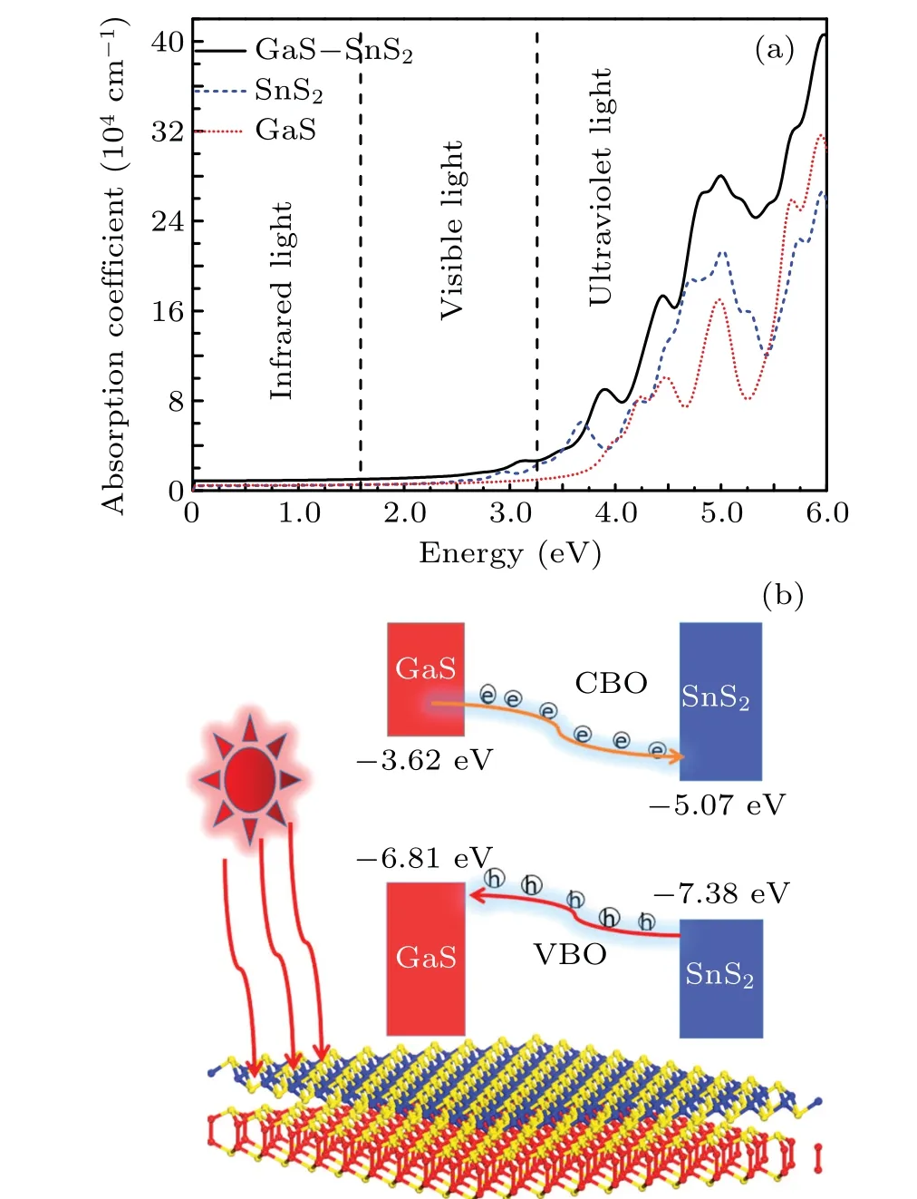
Fig. 9. (a) Absorption spectra of GaS-SnS2 heterostructure and (b)schematic migrating carrier.
A schematic plot to depict the dynamic process of photogenerated carrier at the GaS-SnS2interface is shown in Fig. 9(b). In the GaS-SnS2heterostructure, the photogenerated electrons of the GaS layer start to transfer to the SnS2layer in the conduction band,which are motivated by the conduction band offset (CBO) (1.45 eV). Meanwhile, the photogenerated holes move from the valence band of the SnS2layer into the GaS layer, which are driven by a large valence band offset (VBO) (0.57 eV). Hence, the GaS-SnS2heterostructure, exhibiting a type-II band alignment, can be utilized as a photocatalyst.
As is well known,the lifetime of photogenerated carriers is significantly influenced by the build-in electric field.Hence,build-in electric field induced by ground state charge transfer are investigated based on bader charge analysis.[44]The charge transferring from the GaS layer to the SnS2layer is 0.938e, leading to an electric field from the GaS layer to the SnS2layer. This electric field will promote interlayer charge transfer and prohibit carrier recombination, favoring a good light harvesting efficiency.
4. Conclusions
In this work,the electronic and optical properties of GaSSnS2heterostructure have been investigated with density functional theory. It is found that the hexagonal GaS-SnS2heterostructure is a stable semiconductor with a suitable indirect band gap. Interestingly, the GaS-SnS2heterostructure has a type-II band alignment, which is beneficial to photocatalyst.In the GaS-SnS2heterostructure,the charge transferring from the GaS layer to the SnS2layer is 0.938ebased on bader charge analysis, forming a build-in electric field for charge separation.The absorption behavior of GaS-SnS2heterostructure is enhanced in comparison with that of the individual GaS monlayer and SnS2monolayer,indicating that the GaS-SnS2heterostructure is very efficient at absorbing the visible light to expand the application into photocatalyst and opto-electronic devices.
Acknowledgements
Project supported by the National Natural Science Foundation of China (Grant No. 1186040026), the Incubation Project for High-Level Scientific Research Achievements of Hubei Minzu University, China (Grant No. 4205009), and the Fund of the Educational Commission of Hubei Province,China(Grant No.T201914).
- Chinese Physics B的其它文章
- Helium bubble formation and evolution in NiMo-Y2O3 alloy under He ion irradiation
- Dynamics and intermittent stochastic stabilization of a rumor spreading model with guidance mechanism in heterogeneous network
- Spectroscopy and scattering matrices with nitrogen atom:Rydberg states and optical oscillator strengths
- Low-overhead fault-tolerant error correction scheme based on quantum stabilizer codes
- Transmembrane transport of multicomponent liposome-nanoparticles into giant vesicles
- Molecular dynamics simulations of A-DNA in bivalent metal ions salt solution