Digital and analog memory devices based on 2D layered PS3(=Mn,Co,Ni)materials?
2021-05-06 08:55:30GuihuaZhao趙貴華LiWang王力XiKe柯曦andZhiyiYu虞志益
Chinese Physics B 2021年4期
Guihua Zhao(趙貴華), Li Wang(王力), Xi Ke(柯曦), and Zhiyi Yu(虞志益),2,?
1School of Electronics and Information Technology,Sun Yat-sen University,Guangzhou 510006,China
2School of Microelectronics Science and Technology,Sun Yat-sen University,Zhuhai 519082,China
3School of Materials and Energy,Guangdong University of Technology,Guangzhou 510006,China
4School of Chemistry and Chemical Engineering,Neijiang Normal University,Neijiang 641100,China
Keywords: electrochemical metallization memory,memristor,2D materials,neuromorphic computing
1. Introduction
Memristors as an electronic synapse is promising in applications of the next-generation artificial neural network,which has attracted extensive research interest.[1–8]According to the mechanisms, the memristors can be mainly classified into three categories: valence change memories (VCM), thermochemical memories(TCM)and electrochemical metallization memories (ECM).[9,10]ECM-based device consists of a thin film of solid electrolyte sandwiched between two electrodes,one is an active metal layer(Ag or Cu)and the other is an inert metal layer (Au or Pt).[11]The solid electrolyte layer acts as an ionic conductor where the active metal ions can migrate under the electrical field.[12]The conductive filament(CF)of active metal is deposited and dissolved between the electrodes with electrical stimulations, which is associated with redox reaction.[11]This process results in resistive switching (RS)for devices. When the CF bridges the electrodes,a device can enter a low resistance state (LRS), otherwise it is in a high resistance state (HRS). Due to dual resistance states, devices were widely used as binary storages. On the other hand,multiple resistance states make devices promising as an artificial synapse suitable for neuromorphic computing.[13]
A vertical structure is popularly used for ECM-based devices because it occupies less space than a planar structure and can be stacked three dimensionally.[14]Memristors based on 2D materials have many advantages such as lowpower consumption and high-frequency operation and temperature tolerance.[15–17]The 2D materials such as transition metal dichalcogenide(TMD),hexagonal boron nitride(h-BN)and MXene have been used as electrolytes in ECM-based devices.[9,18,19]However, memory devices based on threeelement 2D materials are seldom reported. Some layered MPS3(M=transition metal) materials have ionic conductivity and their single crystals can be exfoliated to a few atomic layers.[20–22]In addition, MPS3compounds are semiconductors or insulators with wide band gaps of 1.3–3.5 eV, which can support large ON/OFF resistance ratios for ECM-based devices.[20]Moreover, the ultra-violet (UV) photodetectors,FETs and ECM-based devices composed of full MPS32D materials may be integrated to perform the combined functions of perception, storage and computing in a system on a chip(SOC).[18,23,24]This SOC is suitable for applications of flexible and intelligent vision systems for UV light images with low latency and low-power consumption. Therefore, it is essential to explore ECM-based devices using layered MPS3materials.
Recently, we reported a memristor based on a layered FePS32D material.[25]This device shows dual modes of resistive switching with digital and analog features, which makes the device suitable for complex neuromorphic system. It implies the potential of 2D MPS3materials working as electrolyte in ECM-based devices. In addition, UV photodetector and FETs of 2D MPS3materials have been widely reported.[26–29]However, the memory devices based on 2D MPS3(M=Mn, Co, Ni) materials have not been reported.This limits the exploration and application of eye-like and brain-like systems based on MPS32D materials. Therefore,it needs further exploration to obtain more knowledge and enrich the diversity which can increase possibility of potential applications for these devices.
In this work, vertical devices with a structure of Ag/MPS3/Au (M=Mn, Co, Ni) are introduced. The bipolar RS behavior with sweep voltages are demonstrated. The synaptic potentiation and depression with both sweep and pulse voltages are shown. The results indicate Ag/MPS3/Au devices are promising as both binary memory and synaptic devices.
2. Experimental detail
2.1. Crystal synthesis
MPS3(M=Mn, Co, Ni) single crystals were grown by the same chemical vapor transport(CVT)method as reported in Ref.[25]. First,high-purity powders of M,P,S and I2were mixed according to the mole ratio of 1:1:3:0.0293. The total mass of M, P and S is 1151.37 mg. Then, the mixed powder was transferred to the bottom of a quartz tube in a glove box filled with inert atmosphere. Next,the quartz tube was sealed under the atmospheric pressure of 0.1 Pa with oxyhydrogen flame. Finally, the tube was put in a two-temperature zone furnace and heated slowly to the target temperatures, 690?C(hot zone)and 620?C(cold zone)which keep for two weeks.Then,the single crystals were obtained.
2.2. Device fabrication
The Ag/MPS3/Au (M=Mn, Co, Ni) cross-point devices were fabricated on a silicon oxide substrate. The fabrication procedure consists of three major steps: definition of a bottom electrode, transfer of an MPS3layer and definition of a top electrode. Both metal layers were obtained by lift-off after patterning and the overlap between the electrodes defines the switch region. The Au/Ti bottom electrode with an enlarged pad was created with a width of 4–5 μm and a thickness of 100/10 nm. Next, an MPS3flake was transferred onto the bottom electrode by polydimethylsiloxane (PDMS)after mechanical exfoliation with Scotch tape under an optical microscope.[30]Lastly, the top Ag electrode with a width of 12–13 μm and a thickness of 120 nm was created using the same fabrication process as bottom electrode. All the patterning was operated by laser direct writing (LDW) photolithography on an exposure machine of uPG501 which has enough precision(0.5μm)for this work and lower cost than electron beam lithography(EBL).All the coating was implemented by electron beam evaporation in a DE400 system.
2.3. Sample characterization
The thicknesses of the MPS3layers of the devices were measured by an atomic force microscope (AFM, NTMDT NTEGRA Spectra). The electrical measurements of a sweep mode were investigated by a source-meter(KEYSIFHT B2912A), and the synaptic measurements by pulse stimulations were performed by the combination the sourcemeter (KEYSIFHT B2912A) and a control system (ENlitech RM15001). The elements of MPS3crystals were observed by an energy dispersive spectrometer(EDS)together with a scanning electron microscope(SEM,HITACHI SU8010).
3. Results and discussion
Layered MPS3(M=Mn, Co, Ni) single crystals have a monoclinic structure with space group C2/m.[20]MPS3layers of hexagonal lattices are weakly bonded together through van der Waals interactions (Fig.1(a)). It is obvious that the as-synthesized MPS3(the nominal atom ratio 1:1:3 is used in the whole paper) single crystals have layered structures and are highly crystalline shown in SEM images(Figs.1(b)–1(c),Figs.S1–S3).
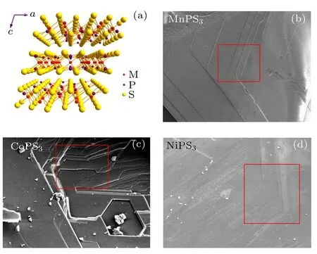
Fig.1. The structure and morphology of as-grown single crystals of MPS3(M=Mn,Co,Ni),the red rectangles indicate the regions for EDS observation.
Vertical Ag/MPS3/Au (M=Mn, Co, Ni) devices were fabricated by the methods described above. As shown in Fig.2(a), an MPS3single-crystalline layer is sandwiched between the Ag top electrode and the Au bottom electrode. The device forms a structure of crossbar where Ag and Au layers show white and yellow colors respectively. The overlap between electrodes define the switch areas, where 2D material layers have single colors with uniform thicknesses(Figs. 2(b)–2(d)). The thicknesses of MnPS3, CoPS3, NiPS3layers are approximately 82 nm(126 layers),93 nm(146 layers)and 114 nm(180 layers),respectively(Figs.S4–S6). The layer number is equal to the thickness of a 2D material divided by the interlayer spacing(see details in Table S1). The crossbar areas are 4×12μm2, 4×12μm2and 5×13μm2for Ag/MnPS3/Au, Ag/CoPS3/Au and Ag/NiPS3/Au devices, respectively.
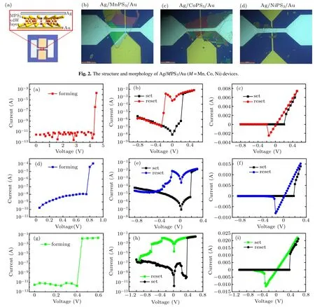
Fig.3. The forming processes and the bipolar behaviors of resistive switching for Ag/MPS3/Au (M=Mn, Co, Ni) devices. [(a), (b), (c)]Corresponding to an Ag/MnPS3/Au device. [(d), (e), (f)] Corresponding to an Ag/CoPS3/Au device. [(g), (h), (i)] Corresponding to an Ag/NiPS3/Au device. [(c),(f),(i)]Linear expressions corresponding to[(b),(e),(h)].
The current-voltage (I–V) curves exhibit behaviors of bipolar RS. Initially, the currents are less than 10?9A at an HRS. Then, the currents jump to over 10?4A and reaches an LRS after the sweep voltages reach the threshold values of 4.25 V, 0.75 V and 0.4 V with a compliance current of 0.1 A (Figs. 3(a), 3(d), 3(g)). After these forming processes,the bipolar RS occurs with applications of positive and negative sweep voltages. When the positive voltages are higher than the thresholds (Vset), the resistance changes from HRS to LRS. On the contrary, the negative voltages turn the resistance from LRS to HRS at the thresholds (Vreset) (Figs. 3(b),3(c), 3(e), 3(f), 3(h), 3(i)). The ON/OFF resistance ratios reach 103, which enables Ag/MPS3/Au devices to be taken as binary memories with high readability. The linear expressions of I–V curves show Ohm behaviors, which implies formation of Ag conductive bridges in the MPS3layers. Moreover, the bipolar characteristics are consistent with the reported Ag2S-based switch, FePS3and CrPS4-based synaptic devices.[25,31–33]Therefore, the RS may be attributed to formation and rupture of Ag conductive bridges, which originate from the Ag ion migration and redox reaction.[11,25,33]It should be noted that the reset processes include more than two RS steps for Ag/CoPS3/Au and Ag/NiPS3/Au devices,which implies the possibility of multi-level RS to be discussed thereinafter. For the Ag/MnPS3/Au and Ag/CoPS3/Au devices,the switching voltages are close to 0.2 V, which is comparable with Cu/MoS2double-layer/Au device that has the lowest switching voltages among 2D materials-based memristors.[34]In addition,the few-layer UV photodetectors based on MnPS3and NiPS3have been reported. The integration of photodetectors and binary memory composed of full 2D materials will enable the device suitable for a flexible and wearable eye-like system in a chip(SOC)with perception and memory functions.[23]
Besides digital RS, Ag/MPS3/Au (M=Mn, Ni) devices also manifest analogue RS behaviors like artificial synapses.For an Ag/NiPS3/Au device,DC sweep voltages were applied to measure the potentiation and depression.When consecutive positive(0 to 0.2 V)and negative(0 to ?0.2 V)sweep voltages were applied,its currents gradually increase and decrease,respectively(Figs.4(a)and 4(b)). This result implies existence of multiple resistance states which can be achieved by sweep voltages. The similar behaviors were also reported for synaptic devices based on MoS2,FePS3,CrPS4and Ag2S.[25,32–34]The conductance is at the level of 100 ?, which means that Ag CFs keep electrodes connected. This analogue RS behavior may be attributed to modulation of overall cross-sectional areas of CFs.[32,34]It is similar for an Ag/MnPS3/Au device.With consecutive application of positive and negative pulse voltages(an amplitude of 0.2 V,a duration of 10 ms,an interval of 50 ms),the resistance decreases and increases between 150 ? and 5000 ?, respectively (Figs. 4(c) and 4(d)). The Ag/MnPS3/Au device also shows multiple resistance states achievable by pulse voltages. The resistance of the Ag atomic contact(12.9 k?)was defined as the threshold of the ON state,according to which the Ag/MnPS3/Au device remains in the ON state with the application of pulse voltages.[32]The resistance was not set back to the initial HRS with the negative pulse voltages. This implies existence of other conductive paths which are not ruptured. The integration of synaptic devices and FETs composed of full MPS32D materials is suitable for a flexible brain-like SOC.[18]
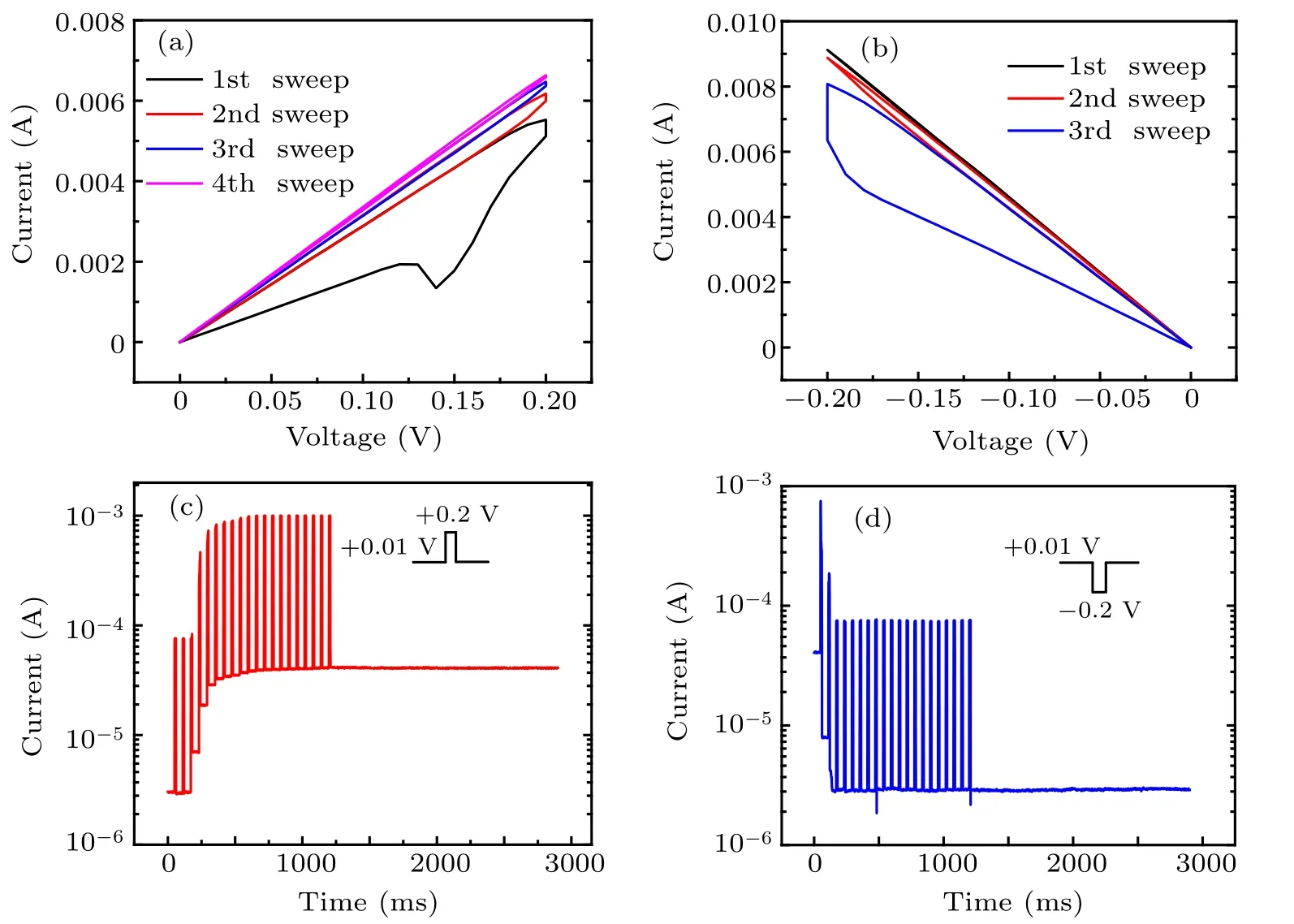
Fig.4.The behaviors of potentiation and depression for Ag/MPS3/Au devices.[(a),(b)]Corresponding to an Ag/NiPS3/Au device with positive and negative sweep voltages between 0 and +0.2 V/?0.2 V. [(c), (d)] Corresponding to an Ag/MnPS3/Au device with positive and negative pulse voltages respectively(amplitude=0.2 V,duration=10 ms,interval=50 ms). The read voltage during the intervals is 0.01 V.
4. Conclusions
In summary, we have demonstrated digital and analogue memory devices with an Ag/MPS3/Au structure based on layered MPS3(M=Mn, Co, Ni) 2D materials. All the devices show bipolar RS behavior. Ag/MnPS3/Au and Ag/NiPS3/Au devices show synaptic characteristics of potentiation and depression. The digital and analog characteristics enable the Ag/MPS3/Au devices suitable for the flexible eye-like and brain-like systems on a chip, especially when they are integrated with photodetectors and FETs composed of full MPS3materials.
Acknowledgement
The authors acknowledge the support by Dr. Yiyan Wang from Institute of Physics,CAS.
- Chinese Physics B的其它文章
- Quantum annealing for semi-supervised learning
- Taking tomographic measurements for photonic qubits 88 ns before they are created*
- First principles study of behavior of helium at Fe(110)–graphene interface?
- Instability of single-walled carbon nanotubes conveying Jeffrey fluid?
- Relationship between manifold smoothness and adversarial vulnerability in deep learning with local errors?
- Weak-focused acoustic vortex generated by a focused ring array of planar transducers and its application in large-scale rotational object manipulation?