Comparing of Inkjet Printing Versus Spin Coating for Preparing Fine Structure Hole Transfer and Emitting Layers in OLED Display Construction
2018-10-26 03:25:36CHENWenbinGUOWenruiMOUWanyingDUZhenzhen
發光學報 2018年10期
CHEN Wen-bin, GUO Wen-rui, MOU Wan-ying, DU Zhen-zhen,
TANG Peng-yu1, SU Wen-ming1, ZHANG Dong-yu1* (1. Printable Electronics Research Centre, Suzhou Institute of Nano-Tech and Nano-Bionics, Chinese Academy of Sciences, Suzhou 215123, China;
2. University of Chinese Academy of Sciences, Beijing 100049, China)*Corresponding Author, E-mail: dyzhang2010@sinano.ac.cn
Abstract: A comparison between the surface properties of inkjet printed and spin coated PEDOT∶PSS films was made in consequence of the intriguing distinction after printing emitting layer inks on them. The sizable and hill-like polymer grains were only found on the surface of the inkjet printed PEDOT∶PSS film. Further investigation demonstrated the difference in morphology stems from the diverse of wetting properties. The differing effects on film properties between inkjet printing and spin coating were revealed, according to which a finer structure was constructed on inkjet printed PEDOT∶PSS film.
Key words: inkjet printing; organic light emitting diodes; multilayer printing; surface morphology control
1 Introduction
Printing technology, including screen printing[1], micro-contact printing[2], and inkjet printing[3-7], have attracted more and more attention because of their obvious superiority in respect to material utilization and cost efficiency. Among them, inkjet printing as the predominant fabrication method has been used in various applications, including healthcare, displays, memories and sensors, showing great promise for future technology[8-10]. To fulfill the requirement of high-speed and small-size printed devices, especially in the application of printing OLED pixels, the underlying morphology controlling the layer application of printed ink is the key. When solution-processed OLED display pixels are constructed, the common procedure is firstly depositing hole injection layer (HIL) or hole transport layer (HTL) by spin coating, and then inkjet-printing the emitting layer (EML)[11-12]. However, spin coating is not a satisfactory process for OLED display pixel fabrication due to the potential harm of forming uneven films inside the pixel as a result of material pileup induced by the intrinsic centrifugal force during spinning[13]. An uneven film will cause nonuniform pixel light emission, which becomes even more severe and unavoidable in the circumstance of large-area substrate. Being different from spin coating, there is no centrifugal force during inkjet printing process, so the undesired material pileup problem could be finely avoided. Besides, spin coating cannot be used to construct multicolor emitting layer with high resolution that otherwise can be simply realized with injet printing[14]. And the material utilization of inkjet printing is higher than that of spin coating[5]. Therefore, multilayer inkjet printing is definitely an excellent choice to fabricate high resolution OLED display.
Nonetheless, it still has a long ride ahead from theory to practice. The most complex thing for multilayer inkjet printing is how to control the interaction and the interface between the printed film and the previously deposited film[11-12,15]. This problem is also a common and bottleneck issue in solution-processed OLED fabrication[16]. When a drop of ink is dripped upon a film surface, the solute of ink tends to gather at the rim of the dot. During drying process, a ring-like morphology forms, which is usually called the coffee ring effect[17]. Although the coffee ring effect has been utilized in some electronic device fields[18-19], it is necessary to be eliminated for achieving uniform films in the printed pixels, which is essential to obtain an increased ratio of light emitting area in every pixel and improved electrical uniformity in OLED display panels[20].
Poly(3,4-ethylenedioxythiophene)∶poly(styrene sulfonate) (PEDOT∶PSS) is widely used as a hole injection layer or hole transport layer in OLEDs as a consequence of its high work function (5.2 eV) and conductivity(130 s/cm in in-plane charge transport)[21-22]. As we know, both the surface quality of the conductive layer and property of the ink together dominate the morphology of drop dots upon the film, although the ink property and corresponding adjustment are also important[12,15]. As a result, the surface property of PEDOT∶PSS film prepared by inkjet printing(IJ) and spin coating(SP) was studied in this work. In detail, several types of small molecule phosphorescent emitting layer ink with different solvent ratio were printed upon IJ and SP PEDOT∶PSS films, respectively. The morphology of all ink dots appeared insensitive to mixture ratio, but the most interesting thing was the distinct dot diameter dependence on the PEDOT∶PSS films. Based on the experimental results and analysis, an uniform printed emitting layer could be achieved on the IJ PEDOT∶PSS film by adjusting the solvent ratio, which has a significant effect on moving inkjet printing forward to replace the commonly used thermal evaporation process in OLED industry.
2 Experiments
2.1 Materials
PEDOT∶PSS(CLEVIOS-PVP Al4083) was purchased from Heraeus. Indan and butoxybenzene were purchased from J&K and used without further purification. ITO glass(glass slide with indium-tin-oxide film) was purchased from Chinese South Glass Holding Co. Ltd. The small molecule host material, 9-[4-(4-carbazol-9-yl-2-methylphenyl)-3-methylphenyl] carbazole (CDBP)[23], and phosphorescent guest material, iridium(Ⅲ) bis(2- phenylquinolyl-N,C2′) acetylacetonate (Ir(bt)2(acac))[24]were purchased from Nichem Fine Technology Co. Ltd. 9 mg CDBP and 1 mg Ir(bt)2(acac) were dissolved in 1 mL of the organic solvent with different mixture ratio of indan and butoxybenzene to prepare the emission layer inks with a concentration of 10 mg/mL. Chemical structures of ingredients are shown in Fig.1 and the ingredients of the inks we used in this
study is listed in Tab.1.

Fig.1 Chemical structures of ingredients of the emitting layer inks

Tab.1 Ingredients of the emission layer inks
2.2 Deposition of PEDOT∶PSS Films and Inkjet Printing of Emission Layer Ink
Prior to deposition of PEDOT∶PSS films, the ITO glass substrates were degreased with solvents and then treated with oxygen plasma for 3 min. PEDOT∶PSS through a 0.45 μm filter was spin coated upon the cleaned ITO substrate with 3 000 r/min for 1 min. Meanwhile an inkjet printer (Jetlab Ⅱ, Microfab Technologies) was used for the printing of also filtered PEDOT∶PSS with a 50 μm-orifice nozzle at ambient temperature. Stable droplets with a diameter of about 60 μm could be formed at a jetting frequency of 1 000 Hz through the adjustment of the waveform and uniform film was deposited by adjusting the drop space and maintaining the stage temperature of 25 ℃. Then the spin coated and inkjet printed PEDOT∶PSS films were annealed at 120 ℃ for 30 min for deep drying. After annealing the PEDOT∶PSS films, we printed emission layer inks with different solvent ratio upon the spin coated and inkjet printed PEDOT∶PSS films respectively. The orifice diameter of the nozzle for printing emission layer inks was 30 μm in order to obtain stable droplets and emission layer dots were formed upon the PEDOT∶PSS. Finally, the samples were transferred into vacuum oven for removing the residual solvent at 80 ℃ for 2 h.
2.3 Characterization
The morphology of the emission layer dots upon the PEDOT∶PSS films was measured with a stylus profilometer(DektakXT, BRUKER). An optical contact angle and interface tension meter (SL150L, Kino) was employed to measure the contact angles of the solvents on the PEDOT∶PSS films by using its pendant drop mode at ambient temperature of 23 ℃ and by single circle fitting method for calculating the exact contact angle. The height and phase diagrams with corresponding average roughness were recorded with the help of a Veeco Dimension 3100 atomic force microscope at ambient temperature in tapping mode.
3 Results and Discussion
Firstly, ink 1 and ink 2 were printed upon the PEDOT∶PSS films. The morphologies of the emission layer dots upon the IJ and SP PEDOT∶PSS films were characterized by stylus profilometer. The results are shown in Fig.2. From Fig.2, as the solvent mixture ratio of n-butoxybenzene increased from 10% to 20%, the shape of dots displayed an imperceptible change on the same film, either for ink 1 or ink 2. It meant that the diameters of the dots printed on IJ and SP samples each maintained almost the same size, which was worth nothing. However, a big difference in the diameter of the dots between IJ and SP samples, 180 μm and 380 μm respectively, was found. This result demonstrated that a finer structure could be constructed on IJ PEDOT∶PSS film than that on the SP reference. This is an important finding for printing display device with high resolution.

Fig.2 Morphologies of dots of ink 1 and ink 2 upon IJ and SP PEDOT∶PSS film
To clarify the difference between IJ and SP PEDOT∶PSS films, the contact angles of indan and n-butoxybenzene on the PEDOT∶PSS films were measured by an optical contact angle and interface tension meter. According to the contact angle data shown in Fig.3, indan could perfectly spread on both IJ and SP PEDOT∶PSS films, so both of the contact angles were measured as 0°. In contrast, the contact angle of 13.841° was recorded when n-butoxybenzene was dripped on the IJ PEDOT∶PSS film, but 0° on SP reference. In other words, n-butoxybenzene could only spread well on SP PEDOT∶PSS film. Therefore, we attribute the greater diameter of the dots to the better wetting property of n-butoxybenzene on the SP film than that on the IJ one. The distinction of the wetting property suggested that inkjet printing and spin coating emit different effects on the film forming process of PEDOT∶PSS.
In order to discover this abnormal phenomenon, the atomic force microscope was used in tapping mode to explore the surfaces of two types of PEDOT∶PSS films. From the height and phase diagrams shownin Fig.4 and Fig.5, sizable and hill-like polymer grains were formed and assembled on the surface of IJ PEDOT∶PSS film, leading to an average roughness (Ra) of 2.40 nm. While there were hardly perceptible polymer grains formed on the surface of the SP PEDOT∶PSS film, only 0.98 nm average roughness was achieved.

Fig.3 Contact angles of indan on the IJ PEDOT∶PSS (a), 0° indan on the SP PEDOT∶PSS(b), 0° n-butoxybenzene on the IJ PEDOT∶PSS(c), 13.841° n-butoxybenzene on the SP PEDOT∶PSS(d).
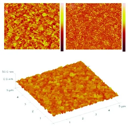
Fig.4 AFM images of the surface of the IJ PEDOT∶PSS film. (a)Height diagram. (b)Phase diagram. (c)3D height diagram.
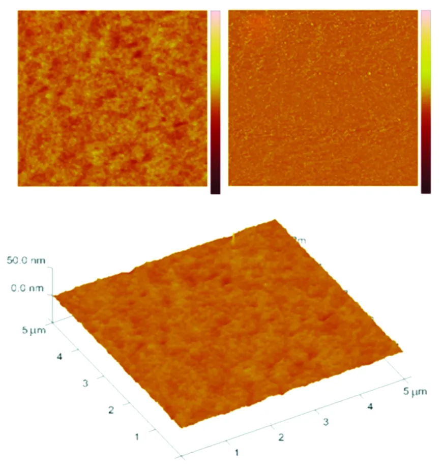
Fig.5 AFM images of the surface of the SP PEDOT∶PSS film. (a)Height diagram. (b)Phase diagram. (c)3D height diagram
Nardesetal. thought that spin coating under high speed generates radial in-plane alignment of flat PEDOT grain structures under the effect of centrifugal forces, which ‘freezes’ under the quick evaporation of solvent[25]. Wilsonetal. proved that convective flow and Marangoni flow inside the inkjet printed drops create columns of transversely elongated and aligned structures or strings of PEDOT grains[26].Therefore, the observed sizable polymer grains on the surface of the IJ PEDOT∶PSS film most likely stem from the transversely elongated PEDOT grains which are quite few in the SP PEDOT∶PSS film.
According to the fact that the different contact angle results were founded only when n-butoxybenzene was used, we prepared the ink 3 in which the n-butoxybenzene was removed. From the morphology of printed ink 3 dot shown in Fig.6, an even emitting layer with restrained coffee ring effect upon IJ PEDOT∶PSS film could be obtained, which is greatly beneficial to our ongoing work of fabricating a multilayer inkjet printing high resolution OLED pixel device. This part of work will be published in elsewhere.

Fig.6 Morphology of dots of ink 3 upon IJ PEDOT∶PSS
4 Conclusion
The major contribution of this study was discovering the reason for the different emitting layer morphologies formed when multilayer printing process was carried on. The emitting layer ink was printed on the surfaces of IJ and SP PEDOT∶PSS films, respectively. Contact angle measurement demonstrated that the morphology difference was derived from the diverse wetting properties. AFM measurement further revealed the existence of sizable and hill-like polymer grains originated from the transversely elongated PEDOT grains on the surface of the IJ PEDOT∶PSS film, but there were quite few for the SP reference. As a result, a finer structure was constructed on IJ PEDOT∶PSS films, which can be used to print the display and other device with high resolution.