The interface of SiO2/ZnS films studied by high resolution X-ray photoluminescence
2018-04-10 08:14:26ShinjitAhryOrlnoTrejoAnupDlniJnTorgersenFilippoBertoFritzPrinz
Shinjit Ahry, Orlno Trejo, Anup Dlni, Jn Torgersen,*, Filippo Berto Fritz Prinz,
aDepartment of Mechanical Engineering, Stanford University, Stanford, CA 94305, USA
bDepartment of Chemistry, Stanford University, Stanford, CA 94305, USA
cDepartment of Mechanical and Industrial Engineering, Norwegian University of Science and Technology, 7034 Trondheim, Norway
dDepartment of Materials Science and Engineering, Stanford University, Stanford, CA 94305, USA
ZnS is an interestingn-type II-VI semiconductor with a wide band gap (3.7 eV), low optical absorption in the visible and infrared spectral regions and high refractive index [1, 2]. ZnS films are widely used in optical and electronic systems in flat panels[3], electroluminescent thin film devices [4], infrared windows[5] and ultraviolet light emitting diodes as well as for buffer layers in solar cells [6, 7].
The deposition of ZnS with atomic layer deposition (ALD) is particularly attractive as this technology provides atomic level thickness [8], and excellent compositional [9] control at relatively low temperatures and mild vacuum conditions. This allows for the precise engineering of the electrical performances of thin films (e.g. recombination [10], resistivity [11], and band alignment [12]). ZnS films can be incorporated in multilayer devices [12, 13] interfacing this metal sulfide to various oxide materials. In such complex architectures proper band alignment is key, which is determined by sharp interfaces [13, 14]. In this aspect, metal-sulfide films present a major challenge due to sulfur’s susceptibility to diffusion [15]. Several researchers have investigated performance and compositional differences of thin films of various thicknesses deposited employing the same process conditions. They hypothesized that these variations are attributed to changes in the chemical environment in the initial cycles of ZnS ALD [7, 12]. To understand this phenomenon, our group has recently employed the element specific capability of X-ray absorption near edge structure (XANES) to investigate the electronic and geometric configuration of various binary and ternary ALD films interfacing metal-oxide substrates [16-19]. We investigated the O K-, S K-edge as well as Zn K and L-edges of thin film ALD ZnS and ZnO1-xSxof various thicknesses interfacing ZnO thin film electrodes [20, 21]. The results indicated the formation of ZnSO4at interfaces, which is known to increase the resistivity and loss in fill factor of the buffer layer [22].
To further understand the importance of this species, we study one particular interface metal-oxide/metal sulfide transition found in CuInxGa1-xSe2(CIGS) based architectures [23]. We investigate the chemical species in the early stages of nucleation on a model substrate (SiO2) as a first step towards a thorough mechanistic study of the ZnS nucleation on oxide substrates.
We used a customized flow-type reactor described elsewhere [24, 25] for the deposition of ALD ZnS. Diethylzinc (DEZ)(Sigma-Aldrich, USA) and H2S gas mixture were used as precursors. The latter contained 3.5% H2S in N2, which resulted in a nonflamable gas mixture. DEZ and H2S were kept at room temperature in 50 cm3stainless steel sample cylinders. The substrate temperature was 160°C. The manifold connecting precursors and the chamber was kept at 100°C. Ten sccm of Ar was flowing through the manifold and acted as the carrier gas adjusting the chamber pressure to 0.6 torr (measured by a Pirani gauge,Lesker, USA). Standard pneumatic ALD valves (Swagelok, USA)were used for pulsing precursor vapour into the chamber. The deposition was carried out on a 500 μm thick p-doped Si <100>wafer. Prior to the deposition of ZnS, the oxide was removed and the cleaned wafer was exposed to 10 H2O pulses inside the ALD chamber (0.1 s pulse, H2O was kept at room temperature in standard 50 cm3cylinders) to ensure the deposition of a 2-3 nm native SiO2prior to the deposition of ZnS avoiding exposure of the wafer to atmosphere. The pulse duration for DEZ was 1 s, for H2S 0.1 s. A growth rate of 0.17 nm/cycle was established (measured by XPS depth profiling and spectroscopic ellipsometry as described in [26, 27]), which was established on this reactor in previous reports [25, 28] and is also reported by others as well within the ALD window [29].
The analysis was conducted in a PHI-Versaprobe (Physical electronics, USA) using Al Kα radiation (1486 eV) in vacuum(5×10⁻¹⁰torr). The instrument was equipped with Ar ion sputter guns for surface cleaning and depth profile analysis. The sample stage could be tilted to increase the surface sensitivity of the analysis.
Figure 1 shows the high resolution XPS peak of S 2p after three complete ALD cycles of DEZ and H2S on a Si<100> wafer with native SiO2surface. The sulfide peaks at 161.2 and 162.2 eV are the binding energies (BE) of ZnS. Due to low signal, it is unclear whether there is spin orbit coupling (fitted like this in Fig.1) or there are indeed 2 species present, where both can be rationalized. At the higher binding energies, there are also 2 peaks fitted, where it is believed that both sulfate and either an intermediate oxidative species or simply noise are present. The presence of interfacial sulfates and intermediate oxidant species is possible because SiO2is flexible in rearranging the surface atoms, which might be more difficult than for other oxide substrates as indicated for TiO2previously [19, 20]. The peaks are also quite broad due to the amorphous nature of the native oxide layer, creating several environments that sulfur is present in.
High resolution XPS (Fig. 2) was also done on a Si wafer that had five complete ALD cycles of H2S and DEZ deposited. The spectra were obtained at different sample mounting angles in order to probe different depths within the sample. At shallow angles, the surface was probed where it is seen that only sulfide species are present. As the angle is increased, the appearance of a sulfate species appears, indicating that the sulfate is located closer to the interface. At an angle almost normal to the analyser(85°), the sulfate species is equal in intensity to the sulfide species, where we are predominantly probing at the interface of the substrate and the ALD ZnS film.
We also conducted a high resolution XPS depth profile of the S 2p peak to further evaluate the confinement of the sulfate species to the interface to the SiO2substrate and that the occurance of the sulfate species is not a matter of exposure of partly exposed substrate to ambient air. This is of particular importance since ZnS and other metal sulfide ALD films exhibit exceptionally strong Volmer-Webber nucleation [28]. When DEZ is introduced, unconnected islands of approximately 5 nm in diameter and a few angstroms in height nucleate over a period of two or three cycles before they coalesce into a continuous film [26]. To ensure that the film was continuous before its exposure to air and to rule out the formation of sulfate species upon exposure to air, a ~170 nm thick ZnS film was grown (100 cycles) and analyzed. The depth profile was done by taking each spectrum after 12 additional seconds of sputtering in succession. Sulfide is only present when no sputtering is done (at top of film). Even after 12 s of sputtering only sulfide is there. After 24 s, we see a sharp decrease in the sulfide peak and a sulfate peak begins to appear.After 36 s and up to 1 min of sputtering, the sulfide peak is practically gone and there is an unmistakable sulfate peak.
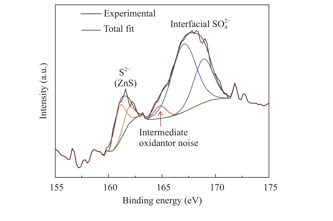
Fig. 1. XPS of S 2p of three complete ALD cycles of H2S and DEZ deposited on Si wafer. It is clearly seen that there are many species present on the surface of the silica. There is sulfur bonded to zinc(ZnS) at the lower binding energies. At the higher energies, it appears as if there are some intermediate oxidants, but mostly interfacial sulfates. The broadness of the higher energy peak suggests that due to amorphous nature of the underlying native oxide, the sulfur is present in many different chemical environments, which may also explain the presence of intermediate oxidant species.
In addition to the S 2p peak that revealed the interfacial presence of sulfate species, the Si 2p peak was tracked in order to find out when the interface was reached. This way, it can be confirmed that the relative intensity of the sulfate species increases(Fig. 3) as the Si signal increases towards the interface (Fig. 4).Indeed, this trend is clearly visible further strengthening the hypothesis that the sulfate species is confined to the interface.
Using standard high resolution XPS, we have shown that an intermediate sulphate is formed upon the exposure of SiO2to the initial cycles of ALD ZnS deposition. Changing the measurement angle of the XPS setup and investigating depth profiles of 170 nm thick ALD films, we rule out the formation of this species resulting from the sample’s exposure to air. Rather, this intermediate species seems inherent to the deposition mechanism. This clearly indicates the need for further studies on application-relevant oxide substrates and extensive mechanistic studies for the fundamental investigation of nucleation mechanism of ZnS and other metal-sulfide ALD processes on oxide substrates, a process that is crucial for many applications in various fields of optoelectronics, where respective thin films are rapidly increasing in popularity.
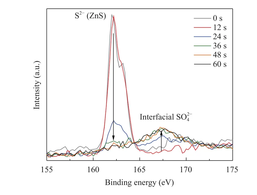
Fig. 3. High resolution XPS of S 2p of 100 complete ALD cycles of H2S and DEZ deposited on Si wafer. A thick sample was necessary to make sure there was no exposed Si interface that when exposed to the environment would result in the formation of a sulfate species.
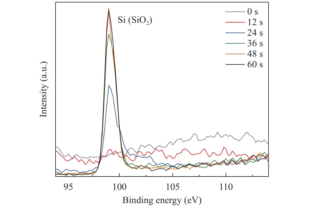
Fig. 4. High resolution XPS of Si 2p of 100 complete ALD cycles of H2S and DEZ deposited on Si wafer.
Acknowledgement
The authors thank the Stanford Nano Shared Facilities(SNSF) for use of PHI VersaProbe Scanning XPS Microprobe for XPS measurements. We gratefully acknowledge partial support from Center on Nanostructuring for Efficient Energy Conversion(CNEEC) at Stanford University, an Energy Frontier Research Center funded by the U.S. Department of Energy, Office of Science, Office of Basic Energy Sciences under Award Number DESC0001060. The Diversifying Academia Recruiting Excellence of Stanford University funded Dr. Orlando Trejo. Dr. Jan Torgersen was funded by the Austrian Research Fund (FWF) under the contract J3505-N20.
[1]K. Benyahia, A. Benhaya, M.S. Aida, ZnS thin films deposition by thermal evaporation for photovoltaic applications, J. Semicond. 36 (2015) 103001.
[2]P. Roy, J.R. Ota, S.K. Srivastava, Crystalline ZnS thin films by chemical bath deposition method and its characterization,Thin Solid Films. 515 (2006) 1912–1917.
[3]B.K. Cha, J.Y. Kim, T.J. Kim, et al., Use and imaging performance of CMOS flat panel imager with LiF/ZnS(Ag) and Gadox scintillation screens for neutron radiography, J. Instrum. 6(2011) C01064.
[4]T. Ishimura, H. Matsumoto, Fabrication of DC inorganic electroluminescent thin-film devices with novel n-p-n type structure, Jpn. J. Appl. Phys. 53 (2014) 042101.
[5]Z. Qu, X. Cheng, R. He, et al., Rapid heating thermal shock behavior study of CVD ZnS infrared window material: Numerical and experimental study, J. Alloys Compd. 682 (2016) 565–570.
[6]K. Ramanathan, M.A. Contreras, C.L. Perkins, et al., Properties of 19.2% efficiency ZnO/CdS/CuInGaSe2thin-film solar cells,Prog. Photovolt. Res. Appl. 11 (2003) 225–230.
[7]A. Hultqvist, C. Platzer-Bj?rkman, E. Coronel, et al., Experimental investigation of Cu(In1-x.Gax)Se2/Zn(O1-z.Sz) solar cell performance, Sol. Energy Mater. Sol. Cells. 95 (2011) 497–503.
[8]C. Bugot, N. Schneider, M. Jubault, et al., Temperature effect on zinc oxysulfide-Zn (O. S) films synthesized by atomic layer deposition for Cu (In. Ga) Se2solar cells, J. Vac. Sci. Technol. A. 33(2015) 01A151.
[9]H.H. Park, A. Jayaraman, R. Heasley, et al., Atomic layer deposition of Al-incorporated Zn(O.S) thin films with tunable electrical properties, Appl. Phys. Lett. 105 (2014) 202101.
[10]M. Igalson, C. Platzer-Bj?rkman, The influence of buffer layer on the transient behavior of thin film chalcopyrite devices, Sol.Energy Mater. Sol. Cells. 84 (2004) 93–103.
[11]U. Malm, J. Malmstr?m, C. Platzer-Bj?rkman, et al., Determination of dominant recombination paths in Cu(In.Ga)Se2thinfilm solar cells with ALD-ZnO buffer layers, Thin Solid Films.(2005) 480–481.
[12]C. Platzer-Bj?rkman, J. Lu, J. Kessler, et al., Interface study of CuInSe2/ZnO and Cu(In.Ga)Se2/ZnO devices using ALD ZnO buffer layers, Thin Solid Films. (2003) 431–432.
[13]S.M. Sze, M.K. Lee, Semiconductor devices, physics and technology, 3rd ed, Wiley, Hoboken, N.J, 2012.
[14]J.H. Davies, The physics of low-dimensional semiconductors:an introduction, Cambridge University Press, Cambridge, U.K. ;New York, NY, USA, 1998.
[15]E. Thimsen, S. V. Baryshev, A.B.F. Martinson, et al., Interfaces and Composition Profiles in Metal-Sulfide Nanolayers Synthesized by Atomic Layer Deposition, Chem. Mater. 25 (2013)313–319.
[16]J.H. Shim, H.J. Choi, Y. Kim, et al., Process-property relationship in high-: K ALD SrTiO3and BaTiO3: A review, J. Mater.Chem. C. 5 (2017) 8000–8013.
[17]J. Torgersen, S. Acharya, A.L. Dadlani, et al., Relating Electronic and Geometric Structure of Atomic Layer Deposited BaTiO3to its Electrical Properties, J. Phys. Chem. Lett. 7 (2016) 1428–1433.
[18]O. Trejo, K.E. Roelofs, S. Xu, et al., Quantifying Geometric Strain at the PbS QD-TiO2Anode Interface and Its Effect on Electronic Structures, Nano Lett. 15 (2015) 7829–7836.
[19]A.L. Dadlani, O. Trejo, S. Acharya, et al., Exploring the local electronic structure and geometric arrangement of ALD Zn(O.S) buffer layers using X-ray absorption spectroscopy, J.Mater. Chem. C. 3 (2015) 12192–12198.
[20]A.L. Dadlani, S. Acharya, O. Trejo, et al., ALD Zn(O,S) Thin Films’ Interfacial Chemical and Structural Configuration Probed by XAS, ACS Appl. Mater. Interfaces. 8 (2016)14323–14327.
[21]A. Dadlani, S. Acharya, O. Trejo, et al., Revealing the bonding environment of Zn in ALD Zn(O.S) Buffer Layers through X-ray Absorption Spectroscopy, ACS Appl. Mater. Interfaces. 9 (2017)39105–39109.
[22]C. Heske, U. Groh, L. Weinhardt, et al., Damp-heat induced sulfate formation in Cu(In.Ga)(S.Se)2-based thin film solar cells, Appl. Phys. Lett. 81 (2002) 4550–4552.
[23]G.-R. Uhm, S.Y. Jang, Y.H. Jeon, et al., Optimized electronic structure of a Cu(In.Ga)Se2solar cell with atomic layer deposited Zn(O.S) buffer layer for high power conversion efficiency,RSC Adv 4 (2014) 28111–28118.
[24]S. Acharya, J. Torgersen, Y. Kim, et al., Self-limiting atomic layer deposition of barium oxide and barium titanate thin films using a novel pyrrole based precursor, J. Mater. Chem. C. 4 (2016)1945–1952.
[25]N.P. Dasgupta, J.F. Mack, M.C. Langston, et al., Design of an atomic layer deposition reactor for hydrogen sulfide compatibility, Rev. Sci. Instrum. 81 (2010) 044102.
[26]J.F. Mack, P.B. Van Stockum, Y.T. Yemane, et al., Observing the Nucleation Phase of Atomic Layer Deposition In Situ, Chem.Mater. 24 (2012) 4357–4362.
[27]Y. Erkaya, D. Nminibapiel, K. Aryal, et al., ZnS Films Deposited by ALD for Solar Cell Applications, ECS Trans. 50 (2013) 45–48.
[28]N.P. Dasgupta, H.J. Jung, O. Trejo, et al., Atomic Layer Deposition of Lead Sulfide Quantum Dots on Nanowire Surfaces,Nano Lett. 11 (2011) 934–940.
[29]G. Stuyven, P. De Visschere, A. Hikavyy, et al., Atomic layer deposition of ZnS thin films based on diethyl zinc and hydrogen sulfide, J. Cryst. Growth. 234 (2002) 690–698.
 Theoretical & Applied Mechanics Letters2018年1期
- Theoretical & Applied Mechanics Letters的其它文章
- A first order friction model for lubricated sheet metal forming
- On the generation of drift flows in wall-bounded flows transiting to turbulence Paul Manneville*
- The effect of fiber orientation on fracture response of metallic fiber-reinforced adhesive thin films
- Thermoelastic vibrations in a thin elliptic annulus plate with elastic supports
- Threshold characteristics of short-pulsed loads combined with the ultrasound field causing dynamic delamination of adhesive joints
- Microstructure design to improve the efficiency of thermal barrier coatings