扶手椅型氮化鎵納米管電子結構與傳輸特性的研究
2015-03-23 11:56:25李恩玲趙丹娜王雪文
原子與分子物理學報 2015年2期
李恩玲, 崔 真, 趙丹娜, 趙 濤, 王雪文
(1.西安理工大學理學院, 西安 710048; 2.西北大學信息科學與技術學院, 西安 710068)
扶手椅型氮化鎵納米管電子結構與傳輸特性的研究
李恩玲1, 崔 真1, 趙丹娜1, 趙 濤1, 王雪文2
(1.西安理工大學理學院, 西安 710048; 2.西北大學信息科學與技術學院, 西安 710068)
本文采用密度泛函理論和非平衡格林函數對扶手椅型氮化鎵納米管(n,n)(2≤ n ≤10)的電子結構和輸運性質進行了研究.結果表明,所有的扶手椅型氮化鎵納米管都是間接帶隙半導體,帶隙隨著納米管直徑的增加而增加,并且得到了兩極體系下氮化鎵納米管的電流-電壓曲線.氮化鎵納米管的半導體特性隨著納米管直徑的增加越來越明顯,電子態密度和電子透射光譜都具有脈沖型尖峰并且最大峰值隨著n的增加而增加.這說明電子態密度和電子透射光譜峰在能量范圍內,有較好的對應關系.
氮化鎵納米管; 電子結構; 傳輸特性; 密度泛函理論
1 Introduction
Gallium nitride (GaN) is an excellent wide band gap semiconductor material which has good optical property and thermal stability. It is an ideal material for the production of semiconductor devices such as blue/green light-emitting diode (LED)[1-2], laser diode (LD), and high power integrated circuit(IC)[3].With the development of highly integrated and micro-scale microelectronic devices, nano-electronic devices have become an important development trend of future devices[4-6]. Low-dimensional nanomaterials have more superior performance compared to their bulk materials due to surface effect[7]and quantum size effect[8].The research on the preparation and properties of low-dimensional GaN nanomaterials can provide technical support to the future nano-devices. Then, studies on one-dimensional GaN nano-materials such as GaN nanotubes have attracted a great attention.
As the preparation technology improved, nano-tubular structures of many materials have been successfully synthesized. In 1997, Liliental-Weberetal. observed nanometer-sized tubular defects in GaN bulk materials[9]. In 2003, Goldbergeretal. prepared successfully single-crystal GaN nanotubes arrays using ZnO nanowires as a template[10]. Currently, GaN nanotubes are still at a stage of preparation and characterization. It is still difficult to prepare good quality GaN nanotubes. So there are few studies of their physical properties. But we can understand the physical properties of GaN nanotubes by theory research which is prior to experiment. Theory research can also help us to predict and analyze various properties of materials, which can provide some guidance to future research[11-15].
In this paper, we systematically study the electronic structure and transport properties of armchair GaN nanotubes (n, n) (2≤n≤10) by density functional theory (DFT) and non-equilibrium green′s function (NEGF). First, we set up GaN nano-tube models then optimize structures to get the band structure of nanotubes. Second, build two-probe systems to obtain the current-voltage curves, electronic density of state, and the electronic transmission spectra of armchair GaN nanotubes (n, n) (2≤n≤10).
2 The theoretical model and the calculation method
2.1 The theoretical model
In this paper, properties of GaN nanotubes are calculated in Atomistix Toolkit (ATK). First, the models of nanotubes are built in ATK. Then a primitive cell is taken and arranged periodicity along the tube axis. In this way, a certain length of GaN nanotubes model are established.
All the models are armchairs GaN nanotubes (n, n) (2≤n≤10) with diameters ranged from 0.34 to 1.72 nm. As armchairs nanotubes are similar in the structure, only the models of (2, 2), (5, 5), and (10, 10) GaN nanotubes are shown in Fig.1, dark gray balls represent nitrogen (N) atoms, light gray balls represent gallium (Ga) atoms, while the lines between the ball and the ball represent the N-Ga bond.
After structure optimization, a two-probe system is built for transport calculations on the basis of optimized structures of GaN nanotubes. As shown in Fig.2, the two-probe system is divided into three parts: the left electrode, the right electrode, and the central scattering region. The both ends of the GaN nanotubes are rigidly attached to Au (1 1 1) surface. The big light gray balls represent Au atoms, the gray and black balls represent Ga atoms and N atoms respectively.
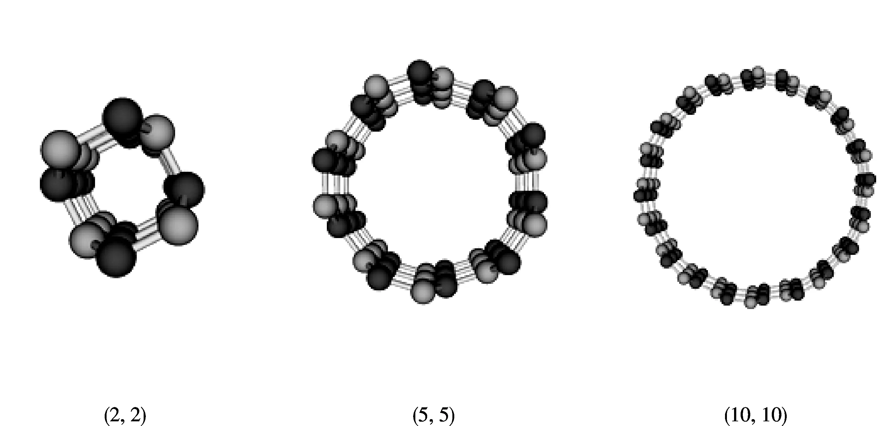
Fig.1 Models of armchairs GaN nanotubes (2, 2), (5, 5), (10, 10)
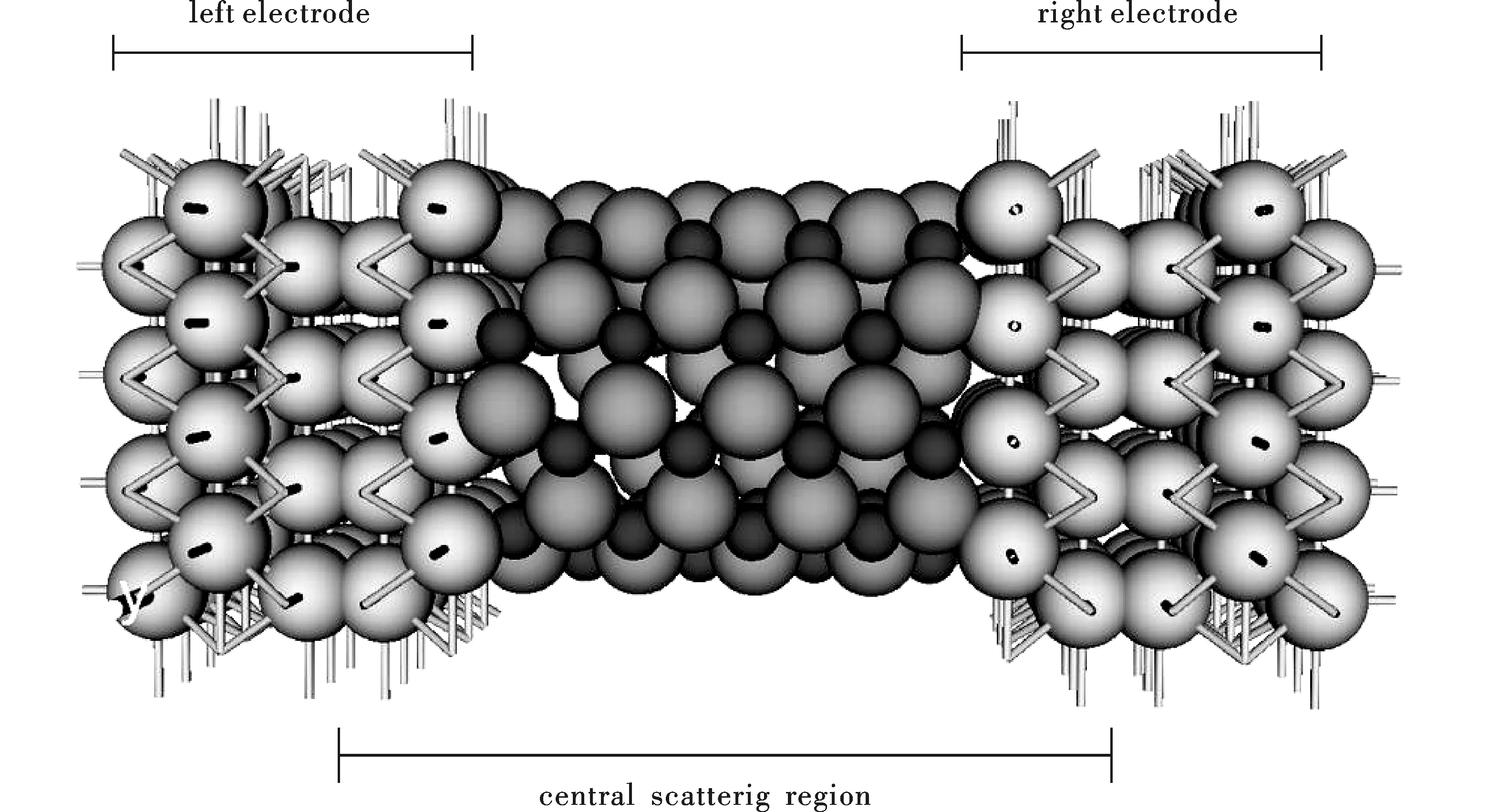
Fig.2 Two-probe system of the armchairs GaN nanotubes
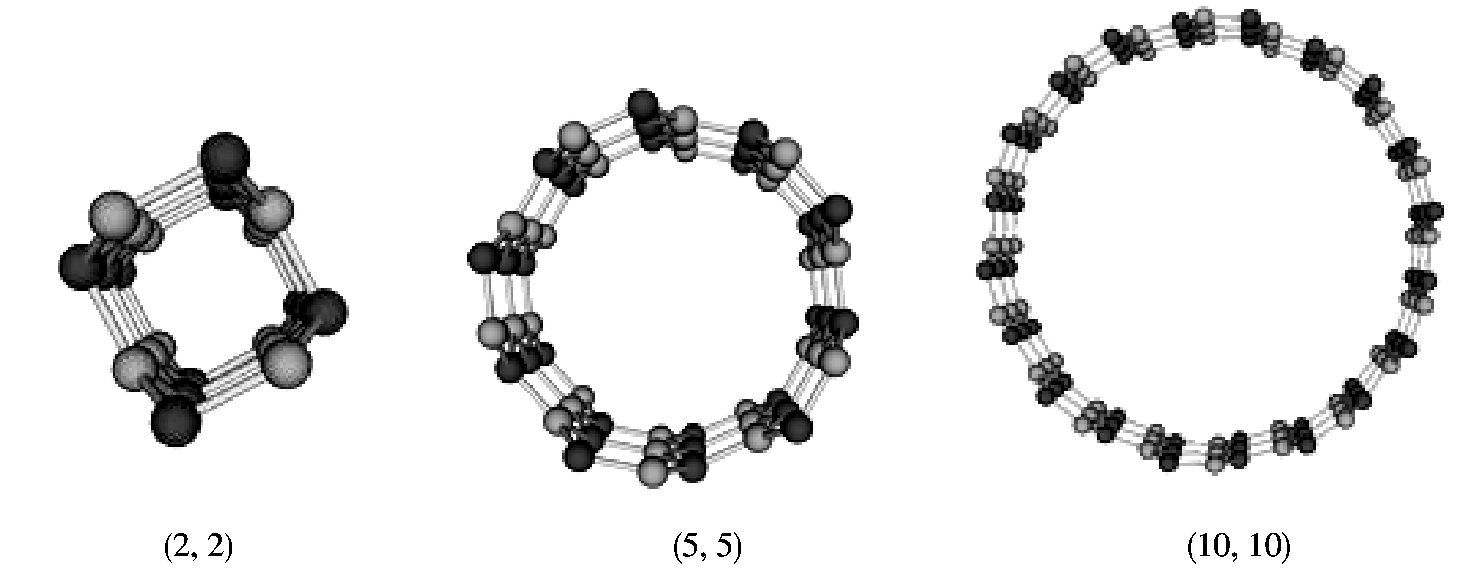
Fig.3 Optimized structures of the armchairs GaN nanotubes
2.2 The calculation method
In this paper, density functional theory (DFT) and non-equilibrium green function (NEGF) are used to calculate the electronic structure and transport properties of single-walled GaN nanotubes. For our calculation, we use a plane-wave based on density-functional (DF) calculation within the local-density approximation (LDA). Exchange-correlation functions parameterized by the Perdew-Zunger scheme are used. The energy cut off for the plane-wave expansion of wave functions is 150 Ry and periodic boundary conditions are applied. Brillouin-zone integral calculations use 1 × 1 × 100 special K-points sampling as suggested by Monkhorst and Pack. The maximum force allowed on each atom is 0.05 eV/?, basis set is double zeta polarized. We use ultrasoft potentials to describe the interaction between a valence electron and the ion core. In the transport calculation, the DFT-NEGF simulation parameters are selected. Cut-off energy is 150 Ry, exchange correlation functional is Perdew-Zunger local-density approximation (LDA.PZ) type with single zeta polarized (SZP) basis set. I-V characteristics are calculated by the equation below:
Whereflandfrare the Fermi distribution functions at left and right electrode respectively.T(E,Vb) is the transmission coefficient at energyEand bias voltageVb.
3 Results and discussion
3.1 Structure optimization
From Fig.3, we can see that Ga atoms move inward along the direction of the tube diameter while the N atoms move toward the opposite direction after optimization. But the average diameter of nanotubes increases. For the Ga atoms and N atoms move in the opposite direction, there form a "buckling" phenomenon which is similar to other dualistic nanotubes[16].

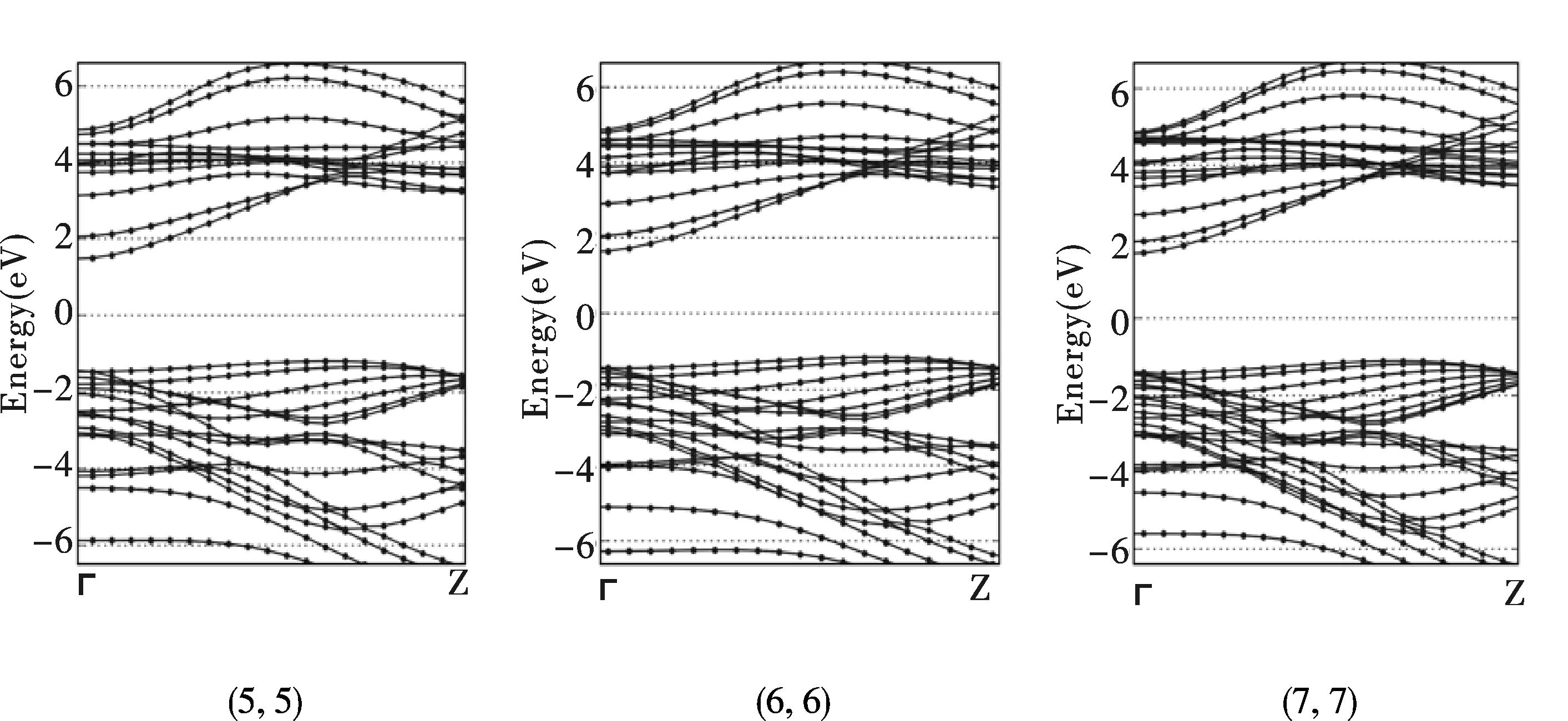

Fig.4 Energy band structures of the armchairs GaN nanotubes
3.2 The energy band structures
The energy band structures of armchairs GaN nanotubes (n, n) (2≤n≤10) are shown in Fig.4 It can be seen that the bottom of conduction band is at the Γ-point, but the top of valence band deviates from the Γ-point, which is about at the 2/3 of Brillouin zone, moves towards the Z-point with n increases. All the nanotubes are indirect band gap semiconductors, which is same as the calculation results of narrow GaN nanotubes by Seung Mi Lee et al[17].
The positions of conduction band bottom, valence band top, and band gaps of the armchairs GaN nanotubes are shown in Table 1. From Table 1, we can see that the conduction band moves up with the increase of n, the top valence band moves down to -1.2294 eV and then moves up. The calculated band gap is from 1.5231 to 2.8787eV and increases with n increases[18]. So the nanotubes we calculated are wide band gap semiconductors. Fig.5 shows the band gap as a function of the tube diameter.
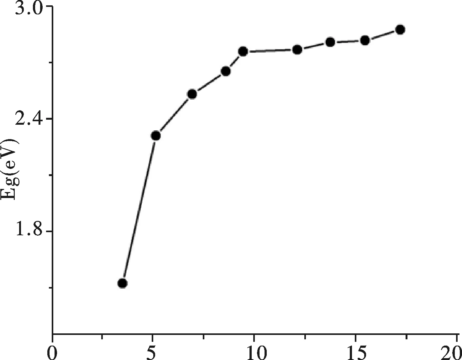
Fig.5 Band gap as a function of the tube diameter

Table 1 Energy values of conduction band bottom, valence band top, band gaps of the nanotubes
3.3 Transport properties
3.3.1Theelectronicdensityofstateandtheelectronictransmissionspectra
The electronic density of state and the electronic transmission spectra of GaN nanotubes with the bias voltage of 0 V on the two-probe system with the armchairs GaN nanotubes are shown in Fig.6. We can see that both the electronic density of state and the electronic transmission spectrums have their own pulse-type sharp peaks. The maximum sharp peak value increases with n increases. There is a better corresponding relation between the peaks energy ranges of electronic density of states and the electronic transmission spectra. This demonstrates that the distribution of electronic transmission spectrum is determined by the distribution of the electronic density of states. The strength of transmission peaks represents the probability size of the electrons pass through central scattering region. If the electron energy is close to the energy of transmission peaks, the electron can be scattered through the nanotubes from left electrode to right electrode[19].
3.3.2Current-voltagecharacteristics
The current-voltage curves of individual nanotubes on two-probe system are calculated with bias voltage range from -2V to 2V and the curves are shown in Fig.7. By curves observing, we find that current increases with voltage increases. Under the same voltage, the currents are increasing with n increasing. The main reason of the current changing trend is that the maxima of sharp peaks in the electronic transmission spectrum and the electronic density of states increase with n increases. All the current-voltage curves of nanotubes are symmetry in the range of -2V to 2V. Each curve has two inflection points which are symmetry. The nanotubes show semiconducting properties due to the existence of the inflection points. The semiconducting properties of nanotubes become increasingly evident with n increases, especially for (8, 8)-(10, 10) nanotubes.
4 Conclusions
We studied the electronic structure of armchairs GaN nanotubes (n, n) (2≤n≤10) using the LDA method based on density functional theory. The band gap is from 1.5231eV to 2.8787eV, all the armchairs GaN nanotubes are indirect band gap semiconductors. The band-gaps increase with the increase of nanotubes diameters.
Transport properties of GaN nanotubes on a two-probe system have been investigated by using density functional theory (DFT) and non-equilibrium green′s function (NEGF). Both the electronic density of state and the electronic transmission spectra have pulse-type sharp peaks and there is a remarkable corresponding relationship between their peaks energy ranges. The maximum values of the peaks increase as the n increases. The current-voltage curves of nanotubes on two-probe system show that the semiconducting properties of nanotubes become increasingly obvious.
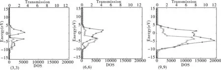

Fig.6 Electronic density of state and the electronic transmission spectra (the dark curve represents the electronic transmission spectra and the light curve represents the density of states)

Fig.7 Current-voltage characteristics of GaN nanotubes on two-probe system
[1] Kyun M Y, Yang K Y, Byeon K J,etal. Enhancement of light extraction in GaN based LED structures using TiO2nano-structures [J].Solid.State.Electron., 2010, 54: 484.
[2] Honga E J, Byeona K J, Parka H,etal. Fabrication of moth-eye structure on p-GaN layer of GaN-based LEDs for improvement of light extraction [J].Mater.Sci.Eng. B, 2009, 163: 170.
[3] Vitanov S, Palankovski V, Maroldt S,etal. High-temperature modeling of AlGaN/GaN HEMTs [J].Solid.State.Electron., 2010, 54: 1105.
[4] Schrimpfa R D, Fleetwoodm D M, Alles M L,etal. Radiation effects in new materials for nano-devices [J].Microelectron.Eng., 2011, 88: 1259.
[5] Dima A, DellaCorte F G, Williams C J,etal. Silicon nano-particles in SiO2sol-gel film for nano-crystal memory device applications [J].Microelectron.J., 2008, 39: 768.
[6] Hong S H , Bae B J, Lee H,etal. Fabrication of high density nano-pillar type phase change memory devices using flexible AAO shaped template [J].Microelectron.Eng., 2010, 87: 2081.
[7] Baron B, Altus E, Tadmor E B . Surface effects in non-uniform nanobeams: Continuum vs. atomistic modeling [J].Int.J.Solids.Struct., 2010, 47:1243.
[8] Condrea E, Nicorici A. Quantum size effect in the resistivity of bismuth nanowires [J].Solid.State.Commun., 2010, 150: 118.
[9] Weber Z L, Chen Y, Ruvimov S. Formation mechanism of nanotubes in GaN [J].Phys.Rev.Lett., 1997, 79(15): 2835.
[10] Goldberger J, He R, Zhang Y,etal. Single-crystal gallium nitride nanotubes[J].Nature, 2003, 422: 599.
[11] Matsunaga R, Matsuda K, Kanemitsu Y. Observation of charged excitons in hole-doped carbon nanotubes using photoluminescence and absorption spectroscopy [J].Phys.Rev.Lett., 2011, 106(3): 037404.
[12] Ebbesen T W, Ajayan P M. Large-scale synthesis of carbon nanotubes [J].Nature, 1992, 358 (6383): 220.
[13] Cabria I, Mintmire J W, White C T. Metallic and semiconducting narrow carbon nanotubes [J].Phys.Rev. B, 2003, 67(12): 121406.
[14] Koh W, Choi J, Lee S G,etal. First-principles study of Li adsorption in a carbon nanotube-fullerene hybrid system [J].Carbon, 2011, 49: 286.
[15] Durgun E, Tongay S, Ciraci S. Silicon and III-V compound nanotubes: Structural and electronic properties [J].Phys.Rev. B, 2005, 72: 075420.
[16] Xiang H J, Yang J L, Hou J G. First-principles study of small-radius single-walled BN nanotubes [J].Phys.Rev. B, 2003, 68(3): 035427.
[17] Lee S, Lee Y, Hwang Y,etal. Stability and electronic structure of GaN nanotubes from density-functional calculations [J].Phys.Rev. B, 1999, 60: 788.
[18] Guo Y H, Yan X H, Yang Y R. First-principles study of narrow single-walled GaN nanotubes [J].Phys.Lett. A, 2009, 373: 367.
[19] Zhao P, Wang P J, Zhang Z,etal. Electronic transport properties of a molecular switch with carbon nanotube electrodes: A first-principles study [J].Phys. B, 2010, 405: 446.
A study on the electronic structures and transport properties of armchairs GaN nanotubes
LI En-Ling1, CUI Zhen1, ZHAO Dan-Na1, ZHAO Tao1, WANG Xue-Wen2
(1. Sciences School, Xi’an University of Technology, Xi’an 710048, China; 2. School Information Technology, Northwest University, Xi’an 710068, China)
Electronic structures and transport properties of armchair GaN nanotubes (n, n) (2≤n≤10) have been investigated using density functional theory (DFT) and non-equilibrium green′s function (NEGF). The results show that all the armchairs GaN nanotubes are indirect band gap semiconductors. The band-gaps increase with the increase of nanotubes′ diameters. The current-voltage curves of GaN nanotubes on two-probe systems have been obtained. The semiconducting properties of GaN nanotubes become more and more obvious with the increasing nanotube diameter. The electronic density of state and the electronic transmission spectra of two-probe system have pulse-type sharp peaks and the maximum values of peaks increase as n increases. There is a better corresponding relation between the peaks energy ranges of electronic density of states and the electronic transmission spectra.
GaN nanotubes; Electronic structures; Transport properties; Density functional theory (DFT)
103969/j.issn.1000-0364.2015.02.009
2013-12-9
國家自然科學基金專項基金項目(51042010);陜西省自然科學基金重點項目(2013JZ018)
李恩玲(1965—),女,陜西咸陽人,博士,教授,主要從事GaN納米材料制備與物性研究. E-mail: Lienling@xaut.edu.cn
O472+.4
A
1000-0364(2015)02-0225-07