3D互連中光刻與晶圓級鍵合技術(shù)面臨的挑戰(zhàn),趨勢及解決方案
2010-01-26 06:05:12MargareteZoberbierErwinHellKathyCookMarcHennemayerDrIngBarbaraNeubert
電子工業(yè)專用設(shè)備 2010年10期
Margarete Zoberbier,Erw in Hell,Kathy Cook,Marc Hennemayer,Dr.-Ing.Barbara Neubert
(1.SUSS MicroTec Lithography GmbH,85276 Garching,Schleissheimerstr.90,Germany;
2.SUSS MicroTec Shanghai Co.,Ltd.Room 3703 Nanzheng Building,580 Nanjing Road West,Shanghai 200041,P.R.China;
3.SUSS MicroTec Inc.,228 Suss Drive,Waterbury Center,VT.05677,USA)
3D互連中光刻與晶圓級鍵合技術(shù)面臨的挑戰(zhàn),趨勢及解決方案
Margarete Zoberbier1,Erw in Hell2,Kathy Cook3,Marc Hennemayer1,Dr.-Ing.Barbara Neubert1
(1.SUSS MicroTec Lithography GmbH,85276 Garching,Schleissheimerstr.90,Germany;
2.SUSS MicroTec Shanghai Co.,Ltd.Room 3703 Nanzheng Building,580 Nanjing Road West,Shanghai 200041,P.R.China;
3.SUSS MicroTec Inc.,228 Suss Drive,Waterbury Center,VT.05677,USA)
目前,3D集成技術(shù)的優(yōu)勢正在擴(kuò)展消費(fèi)類電子產(chǎn)品的潛在應(yīng)用進(jìn)入批量市場。這些新技術(shù)也在推進(jìn)著當(dāng)前許多生產(chǎn)工藝中的一些封裝技術(shù)包括光刻和晶圓鍵合成為可能。其中還需要涂膠,作圖和蝕刻結(jié)構(gòu)。探討一些與三維互連相關(guān)的光刻技術(shù)的挑戰(zhàn)。用于三維封裝的晶圓鍵合技術(shù)將結(jié)合這些挑戰(zhàn)和可用的解決方案及發(fā)展趨勢一并介紹。此外還介紹了一種新的光刻設(shè)備,它可通過圖形識別技術(shù)的輔助實(shí)現(xiàn)低于0.25 μm的最終對準(zhǔn)精度。對于采用光刻和晶圓級鍵合技術(shù)在三維互連中的挑戰(zhàn),趨勢和解決方案及SUSS公司設(shè)備平臺(tái)的整體介紹將根據(jù)工藝要求來描述。在這些技術(shù)中遇到的工藝問題將集中在晶圓鍵合和光刻工序方面重點(diǎn)討論。
三維互連;晶圓鍵合;光刻;解決方案;光刻設(shè)備;鍵合對準(zhǔn)精度;發(fā)展趨勢
The expanding consumer electronics market is clearly driving the development of today's sem iconductor innovation.The push for integration,reduction in power consumption and the need for smaller form factors lead to new architectures which combine dissim ilar technologies and lead to creative packaging methods,where maximum functionality is packaged into minimal space.So 3D Integration is considered the next generation packaging solution.
Today different 3D packaging approaches like SiP(System in Package),SoC(System on Chip)and SoP(System on Package)have been developed in order to answer the requirements for smaller footprint, shorter interconnects and higher performance.
SiP"System in a Package"is a functional system or subsystem w ith multiple w irebonded or flip-chip dies in an IC package.Other components are placed on the motherboard,like passives,SAW/BAW filters, pre-packaged ICs,connectors and Micromechanical parts.This technology enables a stacked chip package w ith reduced form factor.
SoC(System on Chip)integrates all the different functional blocks,like processor,embedded memory, logic core and analog in a monolithic way.These blocks are required to integrate the system design on a single sem iconductor chip.SoC designs usually consume less power and have a lower cost and higher reliability than the multi-chip systems that they replace. And w ith fewer packages in the system,assembly costs are reduced as well.
SoP(System on Package)uses through-vias and high density w iring in order to achieve a higher m iniaturization.It is an emerging Microelectronics technology that places an entire system on a single chip-size package.Where"systems"used to be bulky boxes housing hundreds of components,SoP saves interconnection time and heat generation by enabling a full system w ith computing,communications,and consumer functions all in a single chip[1,2].
Through Silicon Via(TSV)has evolved as one of the key technologies for 3D integration and wafer level packaging.3D TSV has the potential to one day replace w ire bonding and thus enable further size and cost reduction,which is one of the biggest challenges, and increase the performance of the device.
Today 3D TSV technology has become critical to the grow th of 3D components integration,like memory stacking,or for MEMS structure packaging.The first application which is using the TSV as mainstream technology is the packaging of CMOS image sensors(CIS).For CMOS image sensors,WLP is already an industrial reality.Today,already about 35% of CMOS imager sensors can be found into latest consumer cell-phones and notebook cameras are encapsulated in a WL-CSP and this number keeps grow ing (Figure.1.)[3,4].
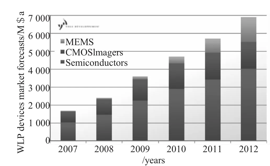
Figure 1 WLP devices market forecasts[4]
1 Process Flow
One of the typical process flows to form TSVs is shown in Figure 2.These steps are required for through silicon via wafer processing.First,the etch mask must be created.This involves coating,exposing and developing the mask.Once the mask is created, the vias can be etched and insulated.Via filling can then be completed using various materials such as copper and tungsten.The fill process is determ ined by the fill materials.As of today,copper is the most commonly used material for TSVs,but other materials like Tungsten(W)or Cu3Sn alloy are used as well.
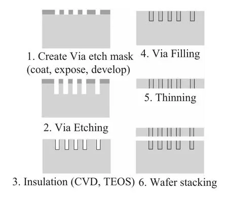
Figure 2 Typical TSV formation flow
2 Process Details
2.1 Exposure and Development
Photolithography of via openings in photo resist looks pretty straight forward.However,the various follow ing process steps and different via sizes require specific photo resist exposure and development conditions and ask for an optim ized set of parameters.
Typically via sizes down to 5 μm(Figure 3)can be easily and cost effectively achieved by 1X full field photolithography.State-of-the-art resolution limits are at about 3 μm in proxim ity printing on 300 mm substrates.However,tight CD control of via openings requires accurate gap setting,excellent light uniform ity and exposure dose control.All this w ill affect the final exposure results and therefore need to be accurately controlled.
For the described experiment a typical via test mask having different via diameters was used.The SUSS MA300 Gen2 Mask Aligner provides an average intensity of about 90 mW/cm?(broadband)coupled w ith a light uniform ity of less than 3%over the whole 300 mm wafer.All wafers were exposed w ith an exposure gap of 20 μm.Figure 3 shows exposed and developed vias w ith a diameter of 3 μm in AZ1505 and further examples.
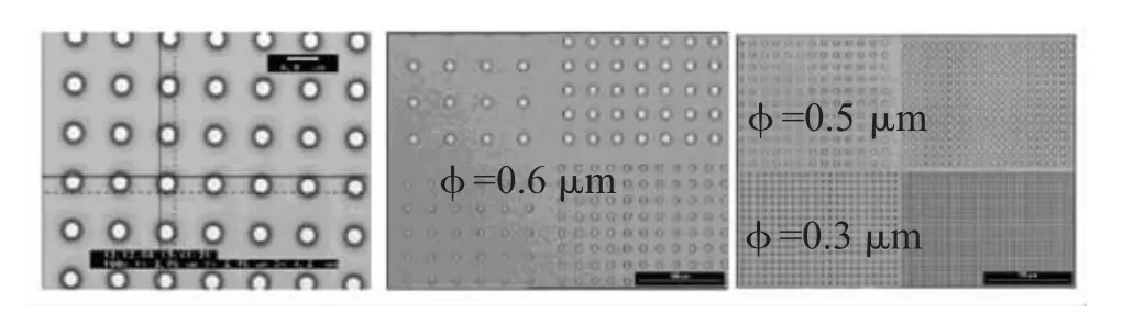
Figure 3 Exposed and developed via w ith a diameter of 3 μm in AZ1505,exposed and developed vias with various sizes(6,5,3 μm)
The development process was again carried out on the ACS300 Gen2 using an aqueous develop module that was equipped w ith a binary spray dispense system.The binary spray nozzle setup and water-jacketed dispense line w ith temperature control to point-of-use allow for reducing process times and m inim izing material consumption.Variable rate arm movement across the wafer was employed in order to optimize the uniform ity of the spray process.Both, AZ4110 and AZ9260 were developed using a 1:4 dilution of AZ400K and deionized water.TMAH based AZ726MIF was used for the development of AZ1505. The trend for smaller vias also requires accurate overlay of the print result.Overall alignment performance of the mask aligner as well as runout effects are the two main important factors that influence the overlay result.The SUSS MA300 Gen2 uses two novel technologies to achieve highly accurate overlay.
Alignment accuracies below 0.5 μm(3sigma) can be achieved on the MA300 Gen2 by adopting the DirectAlign?technology.First of all,the system accurately aligns wafer and mask in alignment gap,which is typically set to 50~100 μm.The final high accuracy alignment step is performed in exposure gap.Advanced pattern recognition software measures and controls the alignment,thus achieving sub-Micron alignment accuracy.
Also alignment accuracies down to 0,25 μm can be achieved now using the MA/BA8 Gen3 Maskaligner.The new Operator-assisted alignment technology w ith continuously automatic calculation of achieved alignment(x,y,θ)between both targets allows extreme alignment accuracy assisted by pattern recognition.During manual alignment the COGNEXRbased pattern recognition software continuously measures the achieved accuracy and reports it to the operator. W ith its sub pixel resolution the Systemsupports highest alignment precision,prevents m isalignment and maximizes yield.So the need for high alignment accuracy is being answered w ith this technology.
Besides an excellent equipment performance in terms of alignment accuracy,the control of mask and wafer temperature is also crucial to achieve optimum overlay results on 300 mm wafers.The MA300 Gen2 employs a temperature controlled exposure chuck to keep a constant and uniform wafer temperature and to compensate for runout effects.In a proxim ity printing system,mask and wafer are in close proximity to each other,assuring that the mask temperature is indirectly controlled by the chuck.Any runout,measured via pattern recognition,can be reduced by changing the temperature in the exposure chuck(Figure 4).The ThermAlignRtechnology is able to reduce runout down to 0.2 to 0.3 μm.

Figure 4 Runout effect between wafer and mask w ith and w ithout temperature control
During the experiment the ThermAlignRchuck was set to 22℃.The alignment was done using an automatic alignment system in direct alignment mode w ith SUSS proprietary alignment targets.
The achieved overlay data on 300 mm wafer are shown in table I and the x-y plot is shown in Figure 5.
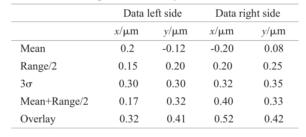
TABLE I A lignment accuracy measurement results
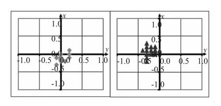
Figure 5 x-y plot of the measurement results
2.2 Bond Alignment
One of the most important topics in 3D Stacking is the alignment accuracy.As can be seen from the roadmap shown in Figure 6,the trend of via sizes is that via diameters w ill continue to shrink over the next couple of years.
Today via diameter in range of 25 to 75 μm are used in CMOS Image Sensors devices.In memory devices typically few Microns diameter is used for a TSV.For the wafer bonding technology,shrinking via diameters have a direct effect on the post bond alignment accuracy that is required.There is always a m inimum overlap requirement so that metal vias have good electrical connection w ith minimized resistance. This m inimum overlap requirement directly translates into post-bond alignment accuracy,which w ill be in the sub-micron range w ithin the next couple of years.

Figure 6 Post-bond Alignment Accuracy Roadmap[4]
As both of the wafers which need to be aligned for 3D stacking have metal layers IR alignment becomes impossible.Another approach is the Inter Substrate Alignment.This technique is capable of achieving the required alignment accuracies outlined in Figure 6.
In this alignment technique special optics are used thatare inserted between the twowafers.The ISA objectives,on left and right,image the alignment key on the upper and lower wafer simultaneously.The alignment stage moves the wafers and a pattern recognition algorithm performsthealignmentaccording to therecipe.
A fter the objectives a re retracted both wafers move into contact or to a predefined gap.Typically moving the wafers in the z-axis can create some m isalignment.Therefore new precision optics and mechanics have been combined w ith global inline calibration methods to achieve sub-Micron alignment accuracy in the BA300UHP(Ultra High Precision)Bond A ligner.
2.3 Bonding
Wafer bonding techniques used for 3D Stacking are mainly:
-metal to metal diffusion bonding(Cu)
-metal eutectic bonding(Cu/Sn)
-silicon fusion bonding
-adhesive bonding(BCB)
There are a lot of pros and cons for each kind of bonding process.Which one w ill be chosen depends on the application and its requirements.However, there is a clear trend for metal to metal diffusion bonding using copper as bond layer.The advantage of this bond process is that the electrical as well as mechanical connection is done simultaneously.
2.3.1 Copper-Copper Bonding
When twometalsarepressed togetherunderapplied force and heat,the atoms can m igrate from lattice site to latticesitebonding the interface together.Such diffusion processes require intimate contact between the surfaces since the atoms move lattice vibration.Copper or Alum inum are optimal for such diffusion processes due to their ductile properties and fast diffusion rates.Copper bondingrequirestemperaturesin therangeof300℃up to 400℃to achieveagood hermetically sealinterface.The oxidation of copper can hamper the bonding process.It canbecracked byapplyingahigh forceduring thebondingor to incorporate a vapor cleaning process to remove the surface oxidation.Using the vapor from formic acid (HC00H)in a bubbler,SUSS MicroTec has developed a pointofuse removalsystem formetaloxides.Wafersare placed in cleaningchambersandexposed to thevapor for a fewm inutes.Thechamber ispurged and by controlling thepartialpressureofO2in themodulenosaltsareformed thatrequiredpostprocessrinses.Theprocessistotallydry and thecoppersurfaceisstableforseveralhours[5].
2.3.2 Metal Eutectic Bonding
Eutectic bonding is also of interest for 3D stacking due to the low temperatures,which are beginning at 231℃for Cu3Sn(Figure 7).Thus the most often requested eutectics are AuSn,AuSi,AlGe,and CuSn, as already mention.It also required the usage of inert gas to prevent oxidation.
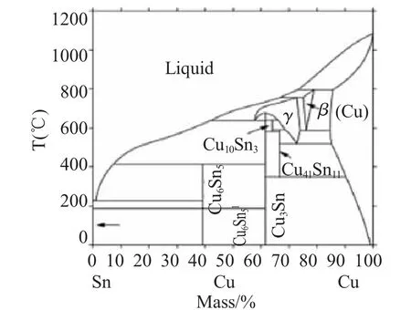
Figure 7 CuSn phase diagramm
2.3.3 Silicon Fusion Bonding
Fusion Bonding is interesting for 3D stacking due to the very short process times and high bond strengths.Nevertheless during the fusion bonding only the mechanical contact is created.However,there are no direct electrical connections across the interface to interconnect the metal layers.Additional processing is therefore required to etch through the wafer stack and backfill vias w ith metals.This is done by thinning one of the substrates to several tens of Micrometers and follow by a patterned etch and metal backfill in a process known as"via last"processing.
Th e drawback to fusion bonding is the requirements for surface flatness and roughness.Another issue is the limitation in the annealing temperature due to the used metal materials in the wafers.But using plasma treatment the annealing temperature canv be reduced from~1 000°down to the required 200℃~400℃.
Silicon fusion bonding needs the follow ing process steps:
-plasma treatment creating a hydrophilic surface w ith a specific chem istry and contact angle
-DI water cleaning combined w ith reactivation and bonding
-temperature annealing in a standard furnace (batch process)
2.3.4 Adhesive Bonding
Adhesive bonding is very often used in 3D due to the low range of process temperature and the topography tolerance.The most often used polymer for precision 3D adhesive bonding is BCB(benzocyclobutene) and is bonded from 150℃-320℃.The flow properties of BCB can be manipulated in order to provide low temperature bonding and alignment accuracies in the range of 1~2 μm.BCB needs to be coated on one or both wafers,the use of adhesive promoter AP3000 is absolutely essential.Before bonding the BCB needs to be baked out.If the procuring is below 150℃not all solvents are removed.So the bond w ill almost certain result in a poor mechanical connection.
I would like to acknow ledge all the co-authors of this paper for their support in creating this paper.
[1]Keith Cooper,Kathy Cook,Bill Whitney.Lithographic challenges and solutions for 3D Interconnects[C].IWLPC,Oct.13-16,2008,San Jose,CA.
[2]Rao R.Tummala.SOP:What is it and why?A new Microsystems-Integration Technology Paradigm-Moore's Law for system integration of miniaturized convergent systems of the next decade[J]IEEE Transactions On advanced Packaging,Vol 27,Nr 2,May 2004,pp 241-249.
[3]3D.Henry,F.Jacquet,M.Neyret.Through Silicon Vias Technology for CMOS Image Sensors Packaging[C]. ECTC,May 27-30,2008,Lake Buena Vista,FL.
[4]Eric Mounier,Jér?me Baron,Jean-Christophe Eloy.A market&technology analysis of WLP solution for IC's[C]. CMOS Image Sensors&MEMS,ECTC,May 27-30, 2008,Lake Buena Vista,FL.
Challenges,Trends and Solutions for 3D Interconnects in Lithography and Wafer Level Bonding Techniques
Margarete Zoberbier1,Erw in Hell2,Kathy Cook3,Marc Hennemayer1,Dr.-Ing.Barbara Neubert1
(1.SUSS MicroTec Lithography GmbH,85276 Garching,Schleissheimerstr.90,Germany
2.SUSS MicroTec Shanghai Co.,Ltd.Room 3703 Nanzheng Building,580 Nanjing Road West,Shanghai 200041,P.R.China
3.SUSS MicroTec Inc.,228 Suss Drive,Waterbury Center,VT.05677,USA)
Technology advances such as 3D Integration are expanding the potential applications of products into mass markets such as consumer electronics.These new technologies are also pushing the envelope of what's currently possible for many production processes,including lithography processesand wafer bonding.
There is still the need to coat,pattern and etch structures.This paper w ill explore some of the lithographic challenges associated w ith 3D interconnection technology.Wafer bonding techniques as used in the 3D Packaging w ill be described w ith all the challenges and available solutions and trends.Furthermore a new Maskalinger technology w ill be introduced which allows extreme alignment accuracy assisted by pattern recognition down to 0.25 μm.
An overall introduction on the challenges,trends and solutions for 3D interconnects in lithography and Wafer Level bonding techniques and the SUSS's equipment platform w ill be described accordingly to the needed processes.The processing issues encountered in those techniques w ill be discussed w ith a focus on wafer bonding and lithography steps.
3D Integration;Wafer Bonding;Lithography;Solutions;Maskalinger;Bonding Alignment Accuracy; Trends
TN405.97
A
1004-4507(2010)10-0026-06
2010-08-25
猜你喜歡
閱讀與作文(英語初中版)(2021年8期)2021-09-13 02:16:29
第一財(cái)經(jīng)(2021年6期)2021-06-10 13:19:08
Coco薇(2017年9期)2017-09-07 21:23:49
少年博覽·小學(xué)低年級(2016年10期)2016-11-24 16:07:01
少年博覽·小學(xué)低年級(2016年9期)2016-11-24 16:07:00
少年博覽·小學(xué)低年級(2016年5期)2016-05-14 11:59:03
紡織服裝流行趨勢展望(2016年2期)2016-05-04 03:47:15
數(shù)字通信世界(2015年10期)2015-12-21 12:22:54
汽車科技(2015年1期)2015-02-28 12:14:44
當(dāng)代體育·扣籃(2014年8期)2014-05-23 13:21:55