Electric modulation of the Fermi arc spin transport via three-terminal configuration in topological semimetal nanowires
2024-01-25 07:14:36GuangYuZhu祝光宇JiAiNing寧紀(jì)愛JianKunWang王建坤XinJieLiu劉心潔JiaJieYang楊佳潔BenChuanLin林本川andShuoWang王碩
Chinese Physics B 2024年1期
Guang-Yu Zhu(祝光宇), Ji-Ai Ning(寧紀(jì)愛), Jian-Kun Wang(王建坤), Xin-Jie Liu(劉心潔),Jia-Jie Yang(楊佳潔), Ben-Chuan Lin(林本川),3,?, and Shuo Wang(王碩),3,§
1Shenzhen Institute for Quantum Science and Engineering,Southern University of Science and Technology,Shenzhen 518055,China
2International Quantum Academy,Shenzhen 518048,China
3Guangdong Provincial Key Laboratory of Quantum Science and Engineering,Southern University of Science and Technology,Shenzhen 518055,China
Keywords: topological semimetal,spin–momentum locking,quantum transport,spin field-effect transistor
Dirac semimetal has received great attention because of its unique quantum transport characteristics, such as higher carrier mobility,[1–4]negative magnetoresistance caused by chiral anomaly,[5–8]as well as extremely large magnetoresistance.[3,9,10]The Dirac semimetal can be transformed into the Weyl semimetal when the time-reversal symmetry is broken.[11]The surface dispersion relation of a Weyl semimetal is topologically equivalent to a non-compact Riemann surface without equal-energy contour that encloses the projection of the Weyl point,[11]leading to the emergence of Fermi arcs,which are a unique topological surface state.[12–17]Fermi arcs have been observed directly by angle-resolved photoemission spectroscopy,which has the characteristic of spin–momentum locking.[18,19]
Spin-momentum locking means the spin of the electrons is locked perpendicular to the carrier’s momentum, as shown in Fig.1(a).This is caused by a strong spin–orbit interaction,which has been observed earlier in the three-dimensional topological insulators,[20,21]as well as the topological Dirac/Weyl semimetals,[18,22–24]through optical and transport measurements.Given that current can induce spin polarization protected by the spin–momentum locking,the electrical detection and control of this key feature are valuable for its application in energy-efficient spintronic devices.[22,25–27]However,previous studies of the spin–momentum locking property in topological materials including topological insulators mostly reported the electric current control of the spin signal, while few reported the electric gate control of the spin signal.Gate control is important because the probable spintronics application would be much more promising if the spin signal can be turned on/off (e.g., a novel type of spin field-effect transistor could be realized).
In this work, spin transport measurements of Dirac semimetal Cd3As2nanowires were carried out using a threeterminal configuration.[28]The resistance demonstrates that a hysteresis loop develops as the external magnetic fields sweep back and forth.A high (low) voltage state is demonstrated when the magnetizationMof the ferromagnetic electrode(Co)is parallel (anti-parallel) to the spin polarizationsof the carriers.This hysteresis resistance state can be reversed by altering the direction of the current,revealing the spin–momentum locking feature of the Cd3As2nanowires.Furthermore, the spin signal can be tuned by the gate voltage, which enables the spin transport on–off states.
The Cd3As2nanowires grown by chemical vapor deposition (CVD) have high quality, large surface volume ratio,and low carrier density.[24,29]Three-terminal geometry measurements were applied for the electrical detection of the spin transport of Cd3As2nanowires.A schematic of the device is displayed in Fig.1(b), in which the ferromagnetic electrode(Co),indicated by blue,is located between the two outer nonmagnetic electrodes (Au), indicated by yellow.The left Au electrode and the middle Co electrode were used to apply current,while the right Au electrode and the middle Co were used to measure the spin signal.The three-terminal geometry was used to separate the current and the voltage circuits, which can limit the anisotropic magnetoresistance[30]and anomalous Hall effect induced by the Co electrodes.[31]An external inplane magnetic fieldBparallel to the long axis of the Co electrode was applied to control the magnetization of the Co electrode.The direction along +yis defined as positive B, while the current along+xis defined as positive.The contacts were patterned via electron beam lithography and were deposited sequentially by electron beam evaporation(EBE).A scanning electron microscopy (SEM) image of the fabricated device is shown in Fig.1(c), in which the Cd3As2nanowire has a diameter of about 150 nm and the width of the ferromagnetic electrode(Co)is 500 nm,while the width of the Au electrodes is 1μm.
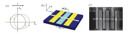
Fig.1.(a)Schematic illustrations of the kx–ky plane of the surface states.Spin is locked to the momentum at each point.(b)The three-terminal geometry measurement diagram,which is used to separate the current and voltage circuits.The middle is a Co electrode indicated by blue and the two outer electrodes are Au electrodes indicated by yellow.(c)The scanning electron microscope image of a typical device.
The three-terminal geometry measurement underT=2 K was carried out and the results are shown in Fig.2.In which a high voltage state and a low voltage state displayed as a hysteresis loop were observed as the external in-plane magnetic field was sweeping back and forth.WhenIdc=100 nA, the momentum carries along the?xdirection (indicated by the black arrow).Due to the spin–momentum locking, the leftmoving electrons have a spin-up polarizationspointing along the +ydirection (indicated by the red arrow), as shown in Fig.2(a).When the magnetization of the Co electrode is+M(indicated by the blue arrow)under a positive field,the relative orientation between electron spinsand+Mis parallel,which leads to a high resistance state.When the field swept from a positive to a negative field, the magnetization of the Co electrode is?M, and therefore electron spinsis anti-parallel to the?Mand a low resistance state was formed.
When the current direction was reversed, i.e.,I=?100 nA,the spin polarization of electronssis also reversed due to the spin–momentum locking (indicated by the red arrow)as shown in Fig.2(b).Therefore,the relative orientation betweensand+Mis anti-parallel under a positive and parallel under a negative field,respectively.As a result,a reversed hysteresis loop signal can be formed,as shown in Fig.2(b).The reversed current leading to the reversed hysteresis loop unambiguously reveals the spin–momentum-locking properties of Cd3As2nanowires.
Furthermore, gate voltageVgtunable measurements[32]were carried out,and the results are shown in Fig.3(a).Here the back gate was applied to the silicon wafer substrate with 285 nm silicon oxide as the dielectric layer.When the applied gate voltage is in the range from?4 V to+4 V,an obvious hysteresis loop signal can be observed.As the voltage increases, the hysteresis loop signal is weakened.When the voltage reached±6 V,the hysteresis loops are vague.Eventually,the spin signals disappeared at a negative voltage of?8 V and a positive+10 V,respectively.
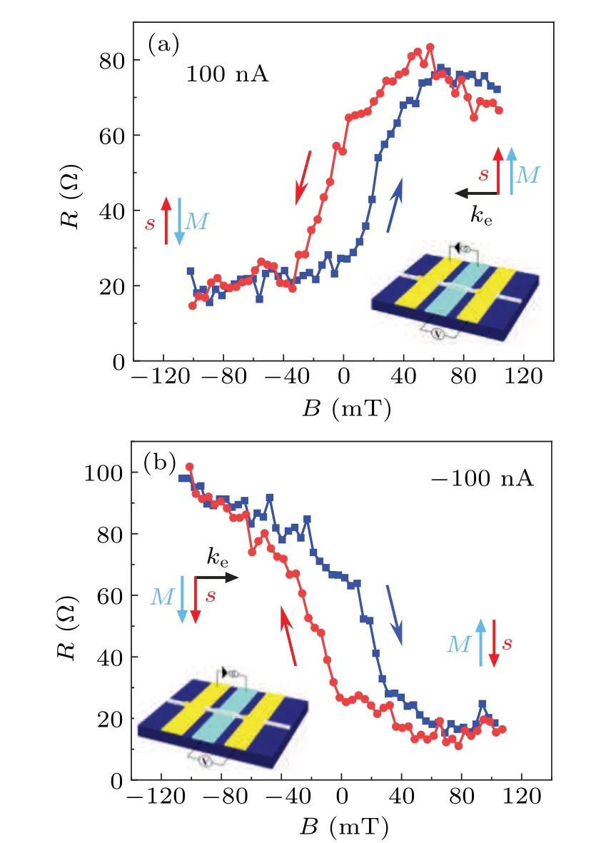
Fig.2.Three-terminal measurement at 2 K.(a) A hysteretic loop signal measured under Idc =100 nA.(b) A hysteretic loop signal measured under Idc =?100 nA.The high resistance states and low resistance states are reversed as the current direction is reversed, showing the spin–momentum locking feature.
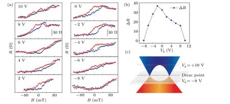
Fig.3.(a)The hysteretic loop signals under various gate voltages.(b)The gate voltage Vg dependence of the height between the high resistance state and the low resistance state.(c)Schematic diagram of the spin signal on–off state under various gate voltages.
To illustrate the gate dependence of the spin signals, we define the height between the high resistance and the low resistance states as ΔR.The extracted ΔRfrom Fig.3(a) as a function of the gate voltage is shown in Fig.3(b).The values of ΔRdisplay a peak atVg=?2 V.As the absolute value of gate voltage increases, the ΔRdecreases.The spin signals are significantly tuned by the gate voltage.Moreover, on–off states can be realized by modulating the gate voltage.The complete on–off spin transport states tuned by the gate voltage enable Cd3As2have great potential in the spin field-effect transistor.The mechanism of the spin signal tuned by gate voltages can be understood as follows.When the Fermi level is close to the Dirac pointVg=?2 V, as shown in Fig.3(c),the spin signal contributed by the Fermi arc reaches its maximum value.When the Fermi level is far from the Dirac point,the contributions from the Fermi arc are weakened,which results in a decrease in the spin signals.When the appliedVgis larger than 10 V orVgis less than?8 V,the spin signals disappear completely.The reason for the complete disappearance of the signal may be attributed to the appearance of a topological phase transition,which is likely to come from the Lifshitz transition.[9–15,17,24]
In summary, we observed a hysteresis loop signal with high resistance and low resistance state through three-terminal geometry measurements, which reveal current-induced spin polarization in the surface state of Dirac semimetals Cd3As2nanowires.Compared to traditional four-terminal configuration, the three-terminal configuration could have a considerably smaller device size in future spintronics applications.The high resistance and low resistance state are reversed while reversing the current direction, which illustrates the spin–momentum locking feature of Cd3As2nanowires.Furthermore,the on–off control of the spin signal can be realized by tuning the gate voltage, which enables the great potential of Cd3As2nanowires in the spin field-effect transistor.Our results provide a new perspective for future spintronic devices.
Acknowledgements
Project supported by the National Key Research and Development Program of China (Grant Nos.2020YFA0309300 and 2022YFA1403700), the National Natural Science Foundation of China (Grant Nos.12004158,12074162, and 91964201), the Key-Area Research and Development Program of Guangdong Province (Grant No.2018B030327001), Guangdong Provincial Key Laboratory (Grant No.2019B121203002), and Guangdong Basic and Applied Basic Research Foundation (Grant No.2022B1515130005).

- Chinese Physics B的其它文章
- High responsivity photodetectors based on graphene/WSe2 heterostructure by photogating effect
- Progress and realization platforms of dynamic topological photonics
- Shape and diffusion instabilities of two non-spherical gas bubbles under ultrasonic conditions
- Stacking-dependent exchange bias in two-dimensional ferromagnetic/antiferromagnetic bilayers
- Controllable high Curie temperature through 5d transition metal atom doping in CrI3
- Tunable dispersion relations manipulated by strain in skyrmion-based magnonic crystals