Intercalation of hafnium oxide between epitaxially-grown monolayer graphene and Ir(111)substrate
2023-10-11 07:56:28YiBiao表奕HongLiangLu路紅亮HaoPeng彭浩ZhiPengSong宋志朋HuiGuo郭輝andXiaoLin林曉
Chinese Physics B 2023年9期
Yi Biao(表奕), Hong-Liang Lu(路紅亮), Hao Peng(彭浩), Zhi-Peng Song(宋志朋), Hui Guo(郭輝), and Xiao Lin(林曉)
University of Chinese Academy of Sciences and Institute of Physics,Chinese Academy of Sciences,Beijing 100190,China
Keywords: epitaxial graphene,hafnium,intercalation,oxidization
1.Introduction
Graphene has attracted extraordinary attention since its discovery.[1]It is one of ideal materials for exploring novel electronic devices because of its unique properties such as high carrier mobility,[2,3]special band structure,[3]etc.Epitaxial growth on metal substrates is a popular method to fabricate high-quality and large-scale graphene.[4–8]However, the electronic structure of graphene can be easily affected by the metal substrates, since the strong interaction between them,which seriously hinders the exploration of its applications especially in electronics.[9,10]To solve this problem, intercalating a buffer layer into the interface between graphene and its substrate, such as small molecules,[11–13]metal atoms,[14,15]and silicon atoms,[16–18]is an effective way to weaken the strong interaction.Moreover,the intercalation of buffer layer can be used to design novel graphene-based heterostructures with clean interfaces.[19,20]
Several studies recently achieved the intercalation of oxide compounds[21,22]between graphene and the corresponding substrates.The dielectric nature of the intercalated layer makes it possible to fabricatein situgraphene/insulator/metal heterostructures[23–26]and measure the transport properties of epitaxial graphene without transfer.Hafnium oxide is widely used in modern electronics because of its high dielectric constant.[27]The intercalation of hafnium oxide is expected to lead to better performances and new applications in graphene-based devices.So far, the successful intercalation of hafnium between graphene islands and metal substrate has been reported.[28]However, intercalation of hafnium below full-layer graphene and corresponding hafnium oxide intercalation still remain challenging.[29]Hence,it deserves further efforts to explore the intercalation and oxidization process of hafnium atoms between full-layer graphene and metal substrate.
In this paper,we investigate the hafnium intercalation and its oxidation process between epitaxial monolayer graphene and Ir(111)substrate.Firstly, large-area monolayer graphene is epitaxially grown on Ir(111) substrate by pre-nucleation method.Subsequently, the hafnium atoms are intercalated to graphene/Ir(111) interface which changes the periodicity of the moiré pattern and keeps the graphene intact,as characterized by LEED and LT-STM.Finally, the interfacial hafnium atoms are oxidized by further oxygen intercalation.Raman characterization confirmed that the hafnium oxide layer effectively decouples graphene from the Ir(111) substrate.Our work explores the intercalation and oxidation of hafnium atoms and provides a platform for applications of epitaxial high-quality graphene.
2.Methods
2.1.Sample preparation
The sample of epitaxial monolayer graphene intercalated with hafnium oxide on Ir(111) substrate was fabricated in an ultra-high vacuum molecular beam epitaxy(UHV-MBE)system with the base pressure of about 5×10⁻¹⁰Torr.The clean surface of Ir(111) substrate was acquired by repeated cycles of sputtering and annealing(1370 K).Epitaxial monolayer graphene was fabricated by exposing the Ir(111)surface to ethylene atmosphere with a pressure of 1×10⁻⁶Torr for 100 sec at the temperature of 1370 K.Hafnium atoms were deposited onto the graphene surface by electron-beam evaporation with the flux of 3 nA for 3 min,and then the sample was annealed at 1270 K for intercalation.The oxidization process was realized by exposing the sample to oxygen with a pressure of 1×10⁻⁵Torr at 570 K.
2.2.LT-STM,LEED,XPS and Raman measurements
Low-temperature scanning tunnelling microscope (LTSTM) used in this experiment is a home-built ultrahigh vacuum system, with a base pressure of about 5×10-11Torr,and allin situmeasurements were carried out in the constantcurrent mode at 4.5 K.Low-energy electron diffraction(LEED) is a commercial SPECS system and thein situcharacterization was carried out at the base pressure of about 5×10⁻¹⁰Torr.X-ray photoelectron spectroscopy(XPS)data were collected via a Thermo Fisher Scientific ESCALAB 250x spectrometer using monochromatic AlKαx-ray source.Raman spectra were obtained by a commercial confocal Raman microscope (WiTec), using an excitation wavelength of 532 nm and a power of 10 mW.
3.Results and discussion
Figure 1 schematically illustrates the procedure of hafnium intercalation and oxidization at the interface between monolayer graphene and Ir(111).The essential step before hafnium intercalation is the epitaxial growth of large-area monolayer graphene on Ir(111)substrate.Due to the weak interaction between graphene and Ir(111)substrate,[30]graphene grown on Ir(111)usually has multi-domain structures.[31]The boundaries between domains will scatter charge carriers and affect the electrical properties of graphene, so it is necessary to epitaxially grow single-domain large-scale monolayer graphene on Ir(111)for high-performance electronic devices.We grow large-scale,single-crystalline graphene by using the pre-nucleation method.We first obtain a clean Ir(111) substrate by using argon ion bombardment and annealing treatment.The substrate has a certain amount of carbon elements in the bulk.After annealing at a high temperature of 1370 K,a small amount of carbon atoms segregate to the surface and form graphene islands.These graphene islands can serve as nucleation sites for the growth of single-domain monolayer graphene.After the second growth process (see details in Section 2), large-scale, high-quality monolayer graphene on Ir(111) is obtained, as shown in Fig.1(a).Then, hafnium atoms are deposited onto the graphene surface and annealed to enable the intercalation (Fig.1(b)).Similar to intercalation of silicon atoms,[32]hafnium atoms intercalate to the graphene/Ir(111)interface through the cooperative interaction mechanism.A subsequent exposure to oxygen leads to the oxidation of intercalated hafnium atoms(Fig.1(c)),and an amorphous HfOxlayer forms between the monolayer graphene and Ir(111)substrate(Fig.1(d)).
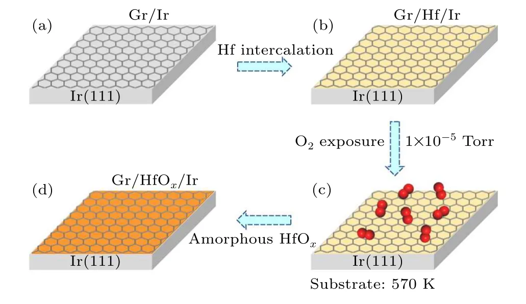
Fig.1.Schematics of hafnium oxide intercalation between monolayer graphene and Ir(111) substrate.(a) Large-scale, high-quality, monolayer graphene on Ir(111) substrate.(b) Hafnium intercalation between graphene and Ir(111) substrate.(c) Oxidation of the interfacial hafnium atoms with O2 partial pressure of 1×10⁻⁵ Torr and substrate at 570 K.(d)Formation of amorphous HfOx between graphene/Ir(111).
To examine the quality of the graphene layer during the whole stages,LEED measurements are employed to characterize structural evolutions.Figure 2(a)shows the sharp Ir(111)spots (indicated by the arrow) which imply the cleanness of substrate before graphene epitaxy.Figure 2(b) is the LEED pattern of the graphene on Ir(111)fabricated by pre-nucleation method, which shows the sharp graphene spots (indicated by the arrow)and surrounding satellite spots due to moiré superstructures between graphene and Ir(111) surface, indicating the graphene is single-crystalline.In Fig.2(b),lrepresents the distance between adjacent diffraction spots of Ir(111)substrate in the LEED pattern, andl1represents the distance between the adjacent moiré spots in the LEED pattern.The ratio ofltol1is~9.32:1.It can be deduced that the moiré period is 2.53 nm,indicating a moiré supercell of epitaxial graphene on Ir(111)substrate contains 10×10 graphene primitive cells and 9×9 Ir(111)primitive cells.After hafnium intercalation,as shown in Fig.2(c), the diffraction spots of graphene are still clear while the satellite spots are blurred, and a new set of diffraction spots appear (indicated by the yellow arrows)which imply the formation of Hf/Ir(111)2×2 superstructure.Moreover, we find that a new moiré structure is formed by graphene and Ir(111) substrate and the period is represented asl2.Compared tol1, the length ofl2becomes larger, and the ratio ofltol2equals to 8.26:1, indicating that the period of moiré superstructure changes to about 2.24 nm.The results confirm a successful intercalation of hafnium atoms below the graphene.After the subsequent oxygen intercalation,only the graphene diffraction spots exist in Fig.2(d)since the amorphous HfOxlayer forms between graphene and Ir(111)substrate.
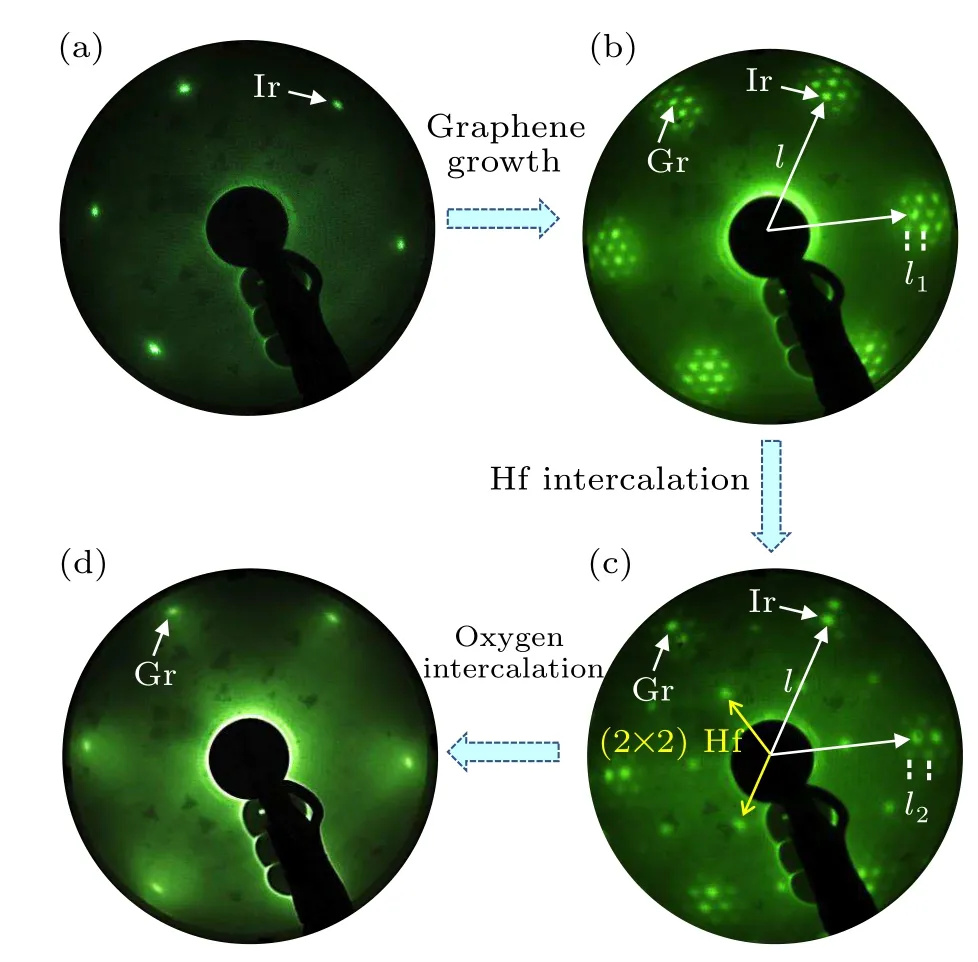
Fig.2.Structure evolutions revealed by LEED patterns after each stage during the hafnium intercalation and oxidation (beam energy: 72 eV).(a)The bare Ir(111)substrate after sputtering and annealing.(b)Largearea, single-crystalline epitaxial monolayer graphene on Ir(111) substrate.(c) Hafnium intercalation between graphene and Ir(111) substrates.(d) Oxygen intercalation to form amorphous oxide layer with the interfacial hafnium atoms.
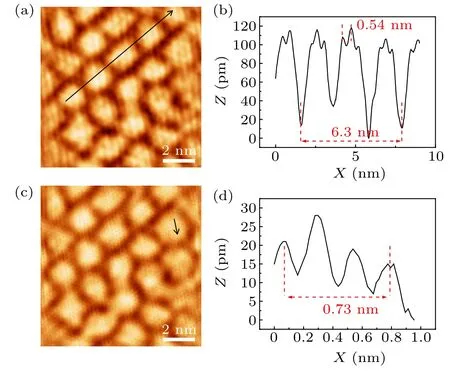
Fig.3.STM topographic images and line profiles of graphene/Ir(111)after hafnium intercalation.(a)STM image(U =-50 mV,I=100 pA)of graphene/Hf/Ir(111) sample, showing the new moiré superlattice and 2×2 superstructure.(b)Line profile along the black arrow in panel(a).(c)STM image(U =-10 mV,I=500 pA)of the same area in panel(a),showing the graphene lattice.(d) Line profile along the black arrow in panel(c).
In order to further study the superstructure formed by hafnium intercalation and the change of graphene moiré periodicity, we use low-temperature STM to characterize graphene/Hf/Ir(111) sample.The STM images in Figs.3(a)and 3(c)show that the surface of graphene is clean,indicating a successful intercalation of hafnium below graphene instead of formation of hafnium clusters on surfaces.In addition,the morphology of graphene has changed, showing different textures from graphene/Ir(111) moiré structure, and the atomic resolution of the graphene honeycomb lattice indicates the intact graphene surface after hafnium intercalation.The line profile in Fig.3(b)along the black arrow indicates that the period of the moiré structure is 2.1 nm, and smaller than the moiré period of graphene/Ir(111),which is consistent with the calculation result from LEED pattern.The period of 2×2 superstructure formed by hafnium intercalation is 0.54 nm, which is exactly two times of the Ir(111) lattice constant 0.272 nm,implying that the 2×2 superstructure is formed by intercalated Hf atoms with respect to Ir(111)rather than stay on the surface of graphene.The line profile in Fig.3(d) along the black arrow indicates the lattice size of the defect-free honeycomb lattice is 0.243 nm, which is consistent with the lattice constant of graphene.Thus,we can confirm that the graphene on the surface remains intact after hafnium intercalation, and the hafnium atoms at the interface form a 2×2 ordered superstructure.
In order to characterize the oxygen intercalated graphene from the macroscopic perspective and examine the effect of oxygen intercalation on the coupling of graphene with the metal substrate, XPS and Raman measurements are performed.The collected Hf 4f core level spectra of graphene/Hf/Ir(111) and graphene/HfOx/Ir(111) by XPS are shown in Fig.4(a).Before oxygen intercalation, Hf 4f peak emerges and exhibits two narrow components due to spin–orbit splitting, corresponding to 4f5/2and 4f7/2, respectively.The peaks of 4f5/2and 4f7/2are centered at 16.0 eV and 14.3 eV.After oxygen intercalation,the peak of 4f7/2is moved to 15.7 eV,suggesting that the hafnium atoms are oxidized.By calculating the peak areas of eigenstate and oxidation peaks of 4f7/2, we confirm that about 80% of the hafnium atoms have been oxidized.Figure 4(b)shows the Raman spectra after oxygen intercalation.The characteristic Raman features of graphene appear, which is different from epitaxial graphene on Ir(111)substrate showing no detectable Raman signals due to the strong hybridization between grapheneπ-band and the Ir(111) substrate, suggesting that the intercalated HfOxlayers effectively decouple graphene from the Ir(111) substrate and the top graphene layer keeps intact.The weak D peak in the Raman curve suggests existence of very few defects in graphene after oxidization.To further examine the quality of the graphene layer after oxygen intercalation, STM is employed to characterize the samples of graphene/HfOx/Ir(111).Figure 4(c)is the large-scale STM image after oxygen intercalation,showing that the topography becomes uneven and indicating the interfacial hafnium has been oxidized to form amorphous structures consistent with the LEED pattern in Fig.2(d).We note that the graphene lattice is still intact after the hafnium and oxygen intercalation,as shown in Fig.4(d).
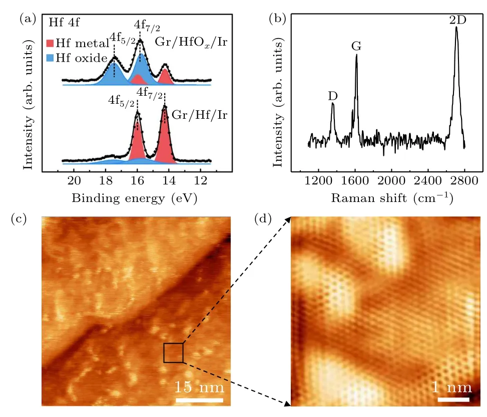
Fig.4.XPS, Raman, and STM characterizations of the graphene/HfOx/Ir(111) sample.(a) Hf 4f core-level spectra of the graphene/Hf/Ir(111) and graphene/HfOx/Ir(111) samples.(b) Raman characterization of the graphene/HfOx/Ir(111)sample.(c)Large-scale STM image (U =-100 mV, I =170 pA) after oxygen intercalation.(d)Zoom-in image(U =-4 mV,I=170 pA)of the area in the black square in panel (c), showing the formation of amorphous HfOx layer,and the top layer is graphene.
4.Conclusion and perspective
We have studied the hafnium intercalation and oxidization process between large-area and high-quality epitaxial monolayer graphene and Ir(111)substrate using LEED,STM,XPS, and Raman characterizations.First, hafnium atoms are intercalated below graphene and form a 2×2 superstructure with respect to Ir(111).The intercalation of hafnium atoms at the interface changes the moiré period of graphene.Then,the graphene/HfOx/Ir(111)structure is realized by oxygen intercalation.The graphene lattice keeps intact after intercalation though amorphous HfOxformed at interface.XPS reveals that about 80% of hafnium atoms have been oxidized.The intercalated layer effectively weakens the interaction between graphene and Ir(111)substrate,since Raman spectra show the characteristic peak of graphene.The successful intercalation of high-kdielectric HfOxlayer provides new opportunities for applications of high-quality graphene in electronic devices.
Acknowledgments
Project supported by the Ministry of Science and Technology of China (Grant Nos.2018YFA0305800 and 2019YFA0308500),the National Natural Science Foundation of China(Grant No.61925111),the Chinese Academy of Sciences (Grant Nos.XDB28000000 and YSBR-003), the Fundamental Research Funds for the Central Universities,and the CAS Key Laboratory of Vacuum Physics.

- Chinese Physics B的其它文章
- Robustness of community networks against cascading failures with heterogeneous redistribution strategies
- Identifying multiple influential spreaders in complex networks based on spectral graph theory
- Self-similarity of complex networks under centrality-based node removal strategy
- Percolation transitions in edge-coupled interdependent networks with directed dependency links
- Important edge identification in complex networks based on local and global features
- Free running period affected by network structures of suprachiasmatic nucleus neurons exposed to constant light