Electronic structure study of the charge-density-wave Kondo lattice CeTe3
2023-10-11 07:56:02BoWang王博RuiZhou周銳XuebingLuo羅學兵YunZhang張云andQiuyunChen陳秋云
Chinese Physics B 2023年9期
Bo Wang(王博), Rui Zhou(周銳), Xuebing Luo(羅學兵), Yun Zhang(張云), and Qiuyun Chen(陳秋云)
Science and Technology on Surface Physics and Chemistry Laboratory,Mianyang 621907,China
Keywords: 4f-electron,charge-density-wave,electronic structure,angle-resolved photoemission spectroscopy
1.Introduction
Investigating the physical connotation of f electrons in heavy fermion (HF) systems is a challenging subject.Consensus exists that the exotic quantum states such as unconventional superconductivity,magnetic order,hidden order and non-Fermi liquid behaviors are all closely related to f electrons in HF systems.[1–3]In HF materials, Kondo entanglement plays a crucial role which is basically manifested by a logarithmic increase of electric resistivity and a following decrease of the resistivity as the heavy quasiparticle emerges with decreasing temperature.The hybridization between f electrons and conduction electrons (f–c hybridization) generates the composite quasiparticles with heavy effective mass and a larger Fermi surface(FS)volume.[4,5]In fact,the f electrons exhibit dual properties, i.e., both localized and itinerant traits.[6,7]They are localized at high temperature and become itinerant as the temperature decreases by hybridizing with conduction electrons.[8,9]Understanding the features of f electrons is significant to explore the origin of the physical properties of HF systems.In this regard,a fundamental and indispensable part is direct observation of the electronic structure,especially the f-electron character,of HF systems.
Many rare earth telluridesRTen(n=2,3)display extraordinary properties,such as charge-density-wave(CDW)transition and pressure-induced superconductivity.[10–13]However,CeTen(n=2, 3) compounds do not turn into the superconductivity state with applied pressure.At ambient pressure,an antiferromagnetic transition temperature is found as low as 4.3 K for CeTe2, while CeTe3is antiferromagnetic belowTN=2.8 K.[14]Besides, CeTe3shows a CDW state at room temperature, however, the transition temperature has never been observed even when the temperature is raised up as high as 500 K.[15,16]
Measurements of transport properties found a weak Kondo lattice behavior below approximately 10 K before CeTe3orders into an antiferromagnetic ground state atTN=2.8 K.This implies the existence of Kondo entanglement in CeTe3at low temperature.[17]Study of CeTe3using nuclear magnetic resonance(NMR)leads to the conclusion that there is coupling between the Te (1) conduction electron band and the Ce local moment, which induces the temperature dependence of the125Te (1) NMR spectrum.CeTe3also has an unconventional CDW interacting between the Ce local moments and the strong Ce spin fluctuations.[18,19]Scanning tunneling spectroscopy (STS) and Raman scattering measurements reveal that the CDW transition opens an energy gap of about 240 meV–740 meV in optimally nested regions on the FS.[20,21]Previous angle-resolved photoemission spectroscopy (ARPES) studies reported multiple shadow bands and FS reconstruction induced by the CDW transition.[10,22]Time-resolved angle-resolved photoemission spectroscopy(tr-ARPES)study reported the collective response of CeTe3in the CDW phase.Momentum-dependent analysis combined with density-functional theory (DFT) frozen phonon calculations reveals different coupling to the band structure for amplitude modes and optical phonons.[23]However, details of the electronic structure,especially how the f electrons interact with the conduction electrons in the CDW state, are still unexplored.Furthermore,the difference in f-electron features in the CDW state and the normal state in other heavy fermion materials also deserves special attention.
In this paper,we explore the electronic structure of CeTe3at different temperatures by ARPES and observe the localized to itinerant transition of f electrons and the opening of an energy gap in one conduction band which is probably related to the CDW state.We also present the electronic structure of CeTe3with different photon energies and polarizations.Measurements with differently polarized light are conducted to distinguish information from different electron orbitals.Meanwhile,with 7 eV and 21.2 eV photons,the fine structure of the bulk and surface states are obtained.
2.Experimental details
High-quality single crystals of CeTe3were grown by the flux method with a mixture of alkali chlorides as the flux.[24]Single-crystal x-ray diffraction(XRD)data,shown in Fig.1(a),were acquired on a PANalytical X’Pert Pro diffractometer (CuKαradiation).As presented in Figs.1(b)–1(d),electrical resistivity and magnetization data were collected by a Quantum Design physical properties measurement system(PPMS).Electrical resistivity was measured based on the fourpoint electrodes method with its ACT module and magnetization measurement was made by a SQUID magnetometer.All ARPES data displayed here except those shown in Fig.6 were obtained at the “Dreamline” beamline of the Shanghai Synchrotron Radiation Facility(SSRF)with a Scienta DA30 analyzer.The energy resolution is 17 meV and angle resolution is 0.2°.The samples were cleaved along thebaxis in ultrahigh vacuum conditions at 18 K before performing ARPES measurements.The base pressure of the system was below 2×10⁻¹⁰mbar during the whole measurement.Laser ARPES and He-lamp ARPES data were collected by the DA30L analyzer and the base pressure was below 8×10-11mbar.The energy and angle resolutions for laser ARPES are 2.5 meV and 0.2°, respectively.The energy and angle resolutions for Helamp ARPES are better than 20 meV and 0.2°,respectively.
3.Results and discussion
The XRD result shown in Fig.1(a) indicates the cleavage plane of the as-grown single crystal is the (010) plane of CeTe3.Meanwhile,the absence of other miscellaneous peaks shows that the quality of CeTe3is fairly good.As shown in Fig.1(b), the electrical resistivity versus temperature curve displays a rather obvious linear behavior from 20 K to 300 K with current flowing in theac-plane.In the range of 3 K to 10 K, there is a plateau where the resistivity nearly remains invariant with decreasing temperature.It is similar to the logarithmic increase with decreasing temperature and may indicate a weak Kondo interaction.[17]Around 3 K,a distinct kink appears which is an indication of the magnetic transition.[25]The residual resistivity ratio (RRR) of these samples reaches 71, implying their good crystal qualities.Figure 1(c) shows the temperature dependence of the susceptibilityχand inverse susceptibility 1/χwith the magnetic fieldH= 0.5 T perpendicular to thebaxis(H⊥b).Above 50 K,1/χdisplays a nearly linear dependence, which is in good agreement with the Curie–Weiss law, and indicates the Ce ions behave in the typical localized model.[26]There is a broad hump below 50 K in the 1/χ–Tcurve.This obvious character may relate to the crystalline-field-effect.[14]Magnetization as a function of the field with the magnetic field perpendicular to thebaxis(H⊥b)at different temperatures is shown in Fig.1(d).At 30 K,a linear lineshape is observed.With decreasing temperature,there is an intermediate state between the linear lineshape and obvious magnetization saturation at 5 K.The saturation susceptibility at 2 K is smaller than that at 3 K.The smaller saturation susceptibility at 2 K is consistent with the trend of resistivity in Fig.1(b)and reveals the possibility of an antiferromagnetic transition below 3 K.[14]
The crystal structure of CeTe3is sketched in Fig.2(a),which shows a layered ABBA stacking order along thebaxis.Here, A stands for the flat Te–Te slabs and the zigzag Ce–Te slabs are described as B.The considerableb/aratio of nearly six reflects its two-dimensional feature.As the gray shaded region between two Te–Te slabs shows, the weak interlayer force makes it easy to form a cleavage surface and the topmost Te atoms are exposed.In such a flat square-net structure, the pxand pzorbitals of the Te atoms hybridize with each other and a square-net electron cloud naturally forms,[27]while the pyorbital perpendicular to the Te–Te layers has a disposition to interact with the electrons of the layers beneath.As Figs.2(b)and 2(c) show, when the bulk crystal structure is considered,the periodicity of Te–Te layers is smaller than the bulk periodicity, leading to the change of the two-dimensional first Brillouin zone(FBZ).We depict the two-dimensional FBZ in Fig.2(d).The dashed black lines reflect the surface state of the topmost Te–Te slab and the solid red lines include the bulk information which is induced by a larger lattice constant mainly resulting from the Ce–Te slabs.The observed FS in Fig.2(e)matches well with the projected BZ calculated with the lattice constants considering the topmost Te–Te slab, while it differs a little from the calculated BZ with the bulk lattice constants.Since CeTe3is a layered structure and easy to cleave,it is possible that the FS contribution is primarily from the Te–Te layer-terminated surface.Meanwhile,a slight contribution from the Ce–Te layers may also exist.The topology of the FS consists of three electron pockets,namely,a square-like electron pocket around theΓpoint, the electron pocket between theΓandMpoints and another electron pocket around theMpoint.In brief, it shows the typical square-net pocket feature and the FS nesting induces CDW formation in CeTe3.[20,22]Detailed band dispersion derived from the photoemission intensity plots along the high-symmetryΓ–MandΓ–Xdirections are shown in Figs.2(f)–2(g).AlongΓ–M, three bands cross the Fermi level, which are marked withα,βandγ, respectively.Two bands marked withεandηare belowEF.The electron-likeγband encloses theΓpoint, forming a squarelike electron pocket around the zone center.The pocket between theΓand M points consists of electron-likeαandβbands.As displayed in Fig.2(g),β,γ,εandηbands can also be clearly observed alongΓ–X, which show similar features to those along theΓ–Mdirection.
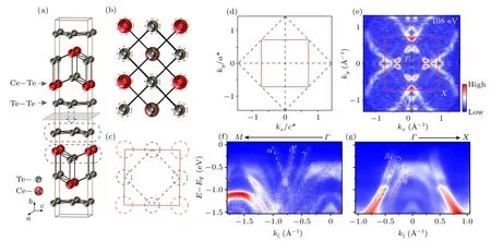
Fig.2.Crystal structure and electronic structure of CeTe3.(a)Crystal structure of CeTe3.Ce and Te atoms are in red and gray,respectively.The shaded area indicates the cleavage plane.(b)Top view of CeTe3 after cleaving.The dotted circles are also shown in panel(c).(c)Positions of Ce(red)and Te(gray)atoms in real space.(d)The Brillouin zone(BZ)of CeTe3.The BZ of the bulk CeTe3 is depicted by the solid red line and BZ of the topmost two-dimensional Te–Te slab is drawn in the dashed black line.(e)Photoemission intensity map of CeTe3 at EF with 108 eV photon energy.The intensity is integrated over a window of[EF-10 meV,EF+10 meV].The setting of the BZ is the same as that in panel(d).(f)–(g)Photoemission intensity distributions along panel(f)Γ–M and panel(g)Γ–X at 18 K.Some typical bands are indicated with colored dashed lines.
To enhance the f-electron photoemission intensity, resonant ARPES measurements were performed at the Ce 4d–4f transition edge with 121 eV photons.Figures 3(a) and 3(b)show the comparison of the ARPES data with on-resonant 121 eV photons and with off-resonant 114 eV photons alongΓ–M.In Fig.3(a), strongly dispersive bands which are centered around theΓandMpoints dominate the off-resonant spectra.Compared with off-resonant photoemission intensity distributions,the on-resonant spectrum reveals three nearly flat bands at binding energies of 0.14 eV, 0.54 eV and 2.95 eV.These flat bands reflect the enhancement of the Ce 4f emission with the on-resonant condition.This is similar to the 4felectron features observed in other Ce-based materials such as CeCoIn5,CeRhIn5and CeIrIn5.[28–30]However,the energy positions of the three flat f bands are further away from the Fermi level compared with other Ce-based compounds;in particular,the position of the f band near the Fermi level is obviously below the Fermi level.The one at 2.95 eV belowEFwith strong intensity can be assigned to the initial 4f0state,while those near 0.14 eV and at 0.54 eV belowEFare from thestate and its spin–orbital coupling (SOC) sidebandcomponent, respectively.[28,31]The flat band at 2.95 eV belowEFderives from the pure charge excitation(4f1→4f0)and is generally known as the ionization peak.[32]And the feature near 0.14 eV is actually the tail of the Kondo resonance aboveEF.We further find the Kondo resonance state exhibits a dispersive characteristic (red dotted line) which can be observed near theMpoint, as shown in Fig.3(d).Moreover,the intensity of thestate is much stronger than that of theand 4f0states.These features indicate the existence of the hybridization between Ce 4f state and the conduction bands.[33]
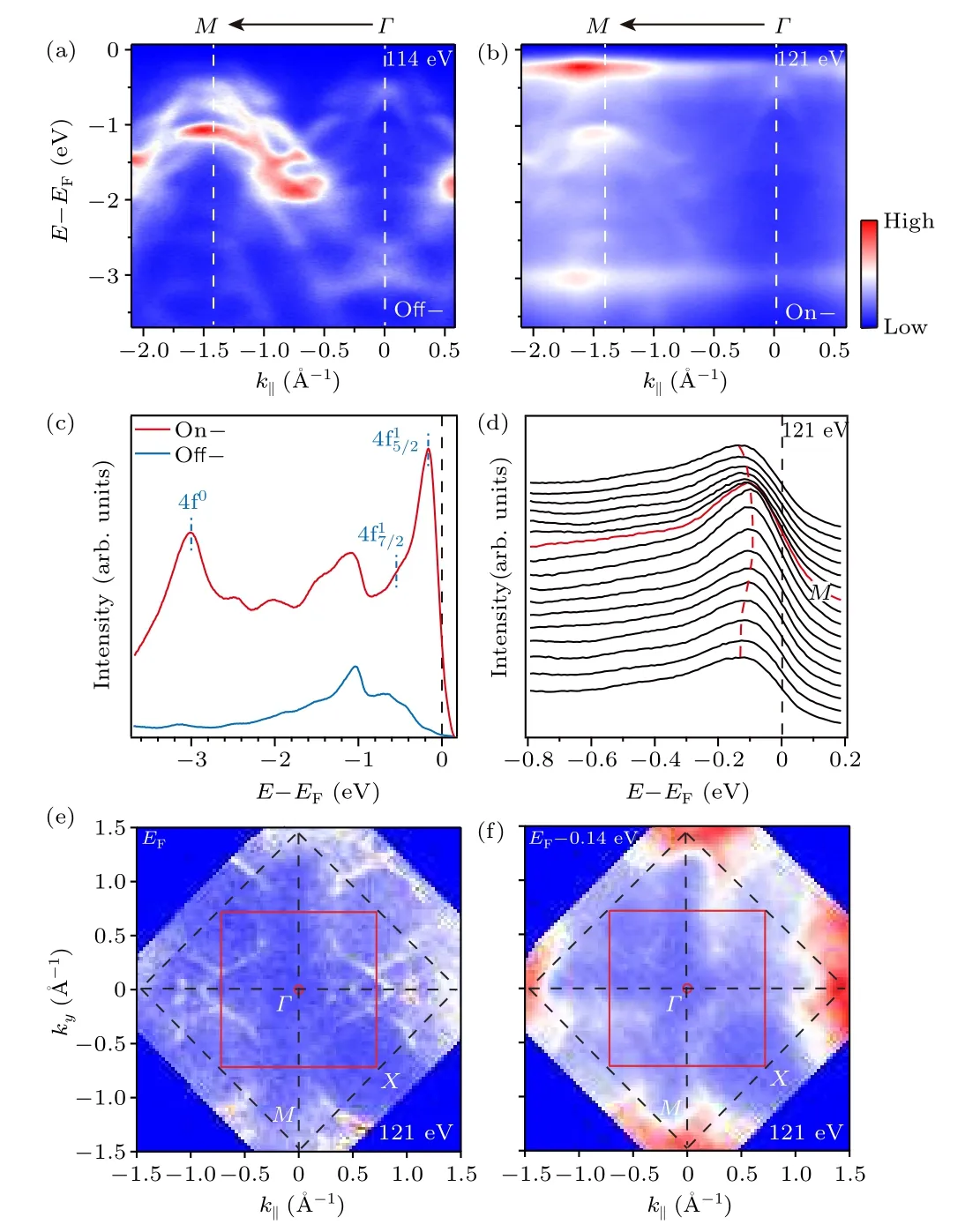
Fig.3.Off/on-resonant ARPES results.(a)–(b)Photoemission intensity distributions of CeTe3 along Γ–M taken at 20 K with (a) off-resonance(114 eV)and(b)on-resonance(121 eV).(c)Angle-integrated energy distribution curves (EDCs) of CeTe3 with on- and off-resonance over the momentum range of [-2.1 ?A-1, -0.7 ?A-1].The f band positions are marked with blue dashed lines.(d) EDCs of CeTe3 with 121 eV photons near the Fermi level.The red solid curve marks the M point and the dashed red curve represents the f band dispersion near the M point.(e)Photoemission intensity map of CeTe3 at EF with 121 eV photons.The intensity is integrated over a window of[EF-30 meV,EF+30 meV].(f)Isoenergetic surface of CeTe3 at 0.14 eV below EF with 121 eV photons.The intensity is integrated over a window of[EF-30 meV,EF+30 meV].
Meanwhile, the spectral intensity of thestate exhibits pronounced momentum dependence.The spectra of the f state centered at theMpoint (red solid curve) in Figs.3(e)and 3(f)show strong intensity,while at other momentum locations, the intensity seems homogeneous and relatively weak.To comprehensively understand the contribution of f electrons to the Fermi surface,a photoemission intensity map atEFwith 121 eV is displayed in Fig.3(e).In comparison with that in Fig.2(e),more f-electron features are observed and the spectral intensity is relatively strong.Moreover, the constant energy surface at 0.14 eV belowEF,where the 4f15/2state is located as shown in Fig.3(f),reveals similar f-electron features but with much stronger spectral intensity.
Figure 4 shows the detailed temperature evolution of the resonant ARPES data alongΓ–Xfrom 25 K to 253 K.From Figs.4(a1)–4(a5), the photoemission intensity is dominated by the strongly dispersive conduction bands.At 0.14 eV and 2.95 eV belowEF, two f-electron band features are obvious.As the red arrow indicates in Fig.4(a1), an energy gap about 0.30 eV is observed in this conduction band.With increasing temperature, the energy gap seems to be closing slowly and detailed information of the gap will be discussed later.In order to clarify the evolution of f-electron with temperature,figure 4(b)displays the temperature dependence of the EDCs nearEFaround theΓpoint.As previously mentioned, the felectron feature nearEForiginates from the 4f15/2state.With increasing temperature,no obvious shift of the peak position is observed,but the change of strength is obvious.The lower the temperature, the stronger the f-electron strength.This shows that with decreasing temperature, f electrons go through the localized to itinerant transition.However, because the peak position of the f states do not show obvious change as shown in Fig.4(b),we propose the f states are not related to the CDW state transition in CeTe3.This is consistent with the high CDW transition of CeTe3.Consequently, the abnormal energy position of the 4f15/2state originates from other reasons, which need further investigations.In addition, the temperature dependence of the energy gap observed in Figs.4(a1)–4(a5) is also shown in Fig.4(c).A conduction band opens an energy gap around theXpoint and the gap is located at about 0.50 eV–0.85 eV belowEF.As the EDCs show in Fig.4(c), with increasing temperature,the strength of the gap decreases and the size of the gap becomes smaller.To explain the change of the energy gap size more clearly,we carried out multipeak fitting processing.In Fig.4(d), it is clear that the size of the gap is mainly about 0.20 eV–0.32 eV and has a negative correlation with temperature.The above phenomenon shows that the gap is gradually closed with the increase of temperature.The behavior in this temperature range is similar to that of CuTe and VTe2,which are also CDW materials,indicating that the existence of the gap may be related to the formation of the CDW state.[34,35]However,since the CDW transition temperature is extremely high and more than 500 K, we cannot observe the closing of the gap at this point.
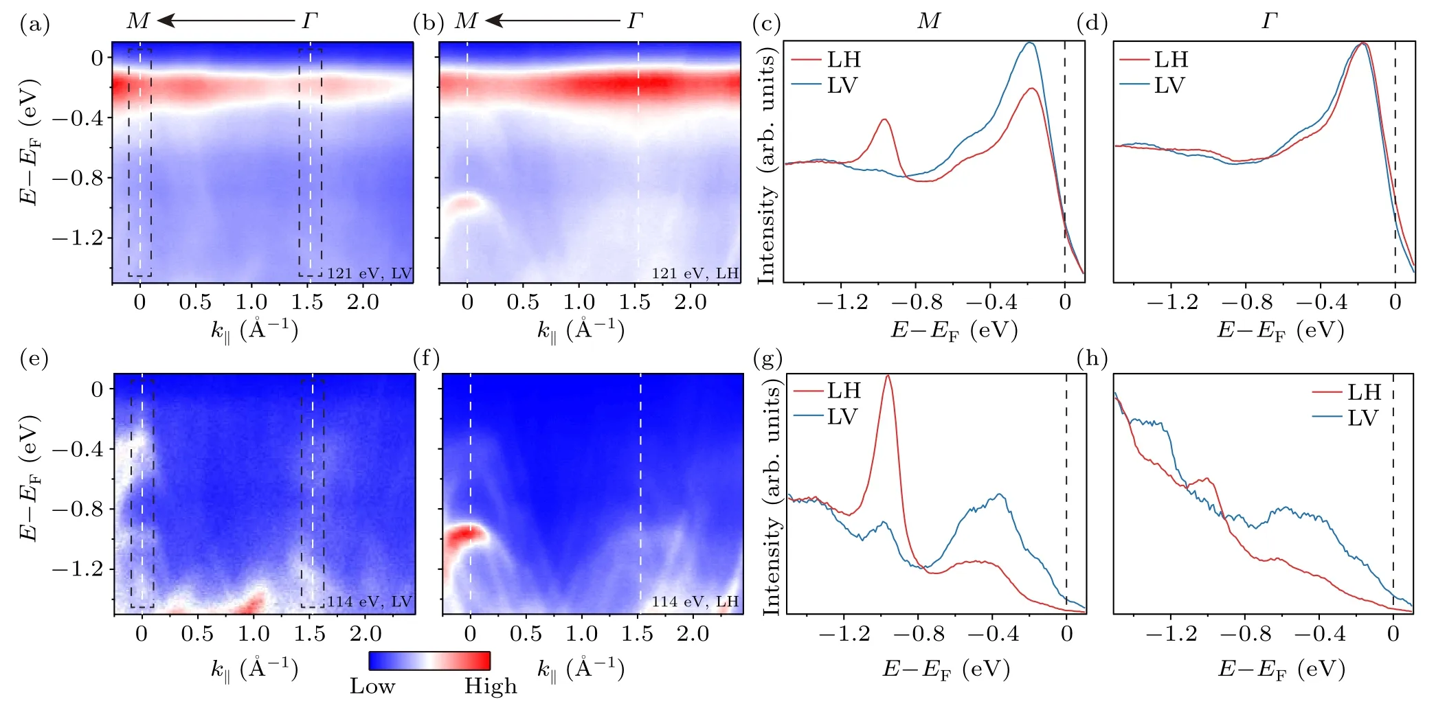
Fig.5.LV- and LH-polarized ARPES results.(a), (b) Photoemission intensity distributions of CeTe3 taken along Γ–M with 121 eV LV- and LH-polarized photons, respectively.(c), (d) Comparison of the angle-integrated EDCs of the black dashed regions in panel (a) with 121 eV LV- and LH-polarized photons, respectively.(e), (f) Photoemission intensity distributions of CeTe3 taken along Γ–M with 114 eV LV- and LH-polarized photons,respectively.(g),(h)Comparison of the angle-integrated EDCs with 114 eV LV-and LH-polarized photons,respectively.The integrated window in panel(e)is marked with the black dashed lines.
To illustrate the effect of different polarized photons on the band structure, LV- and LH-polarized ARPES measurements were further conducted as shown in Fig.5.From Figs.5(a)–5(d),there are three prominent features: (a)the intensity of f bands near the Fermi level with LV-polarized photons is stronger than with LH polarization near theMpoint,but the change of intensity is not apparent near theΓpoint.(b)A hole-like band near theMpoint with LH-polarized photons shows strong dispersion which is located at about 1 eV belowEF, while it is absent with LV-polarized light.(c) The 4f17/2state near theMpoint is enhanced when the polarization is changed from LH to LV, while the state near theΓpoint does not show significant difference with the light.The anisotropy of the orbitals may be a pivotal factor that induces the above phenomena.The variations of the f band and the band at 1 eV belowEF(see more apparent in panels (e)–(h))with different polarized photons display obvious discrepancy,which indicates diverse orbital symmetries.
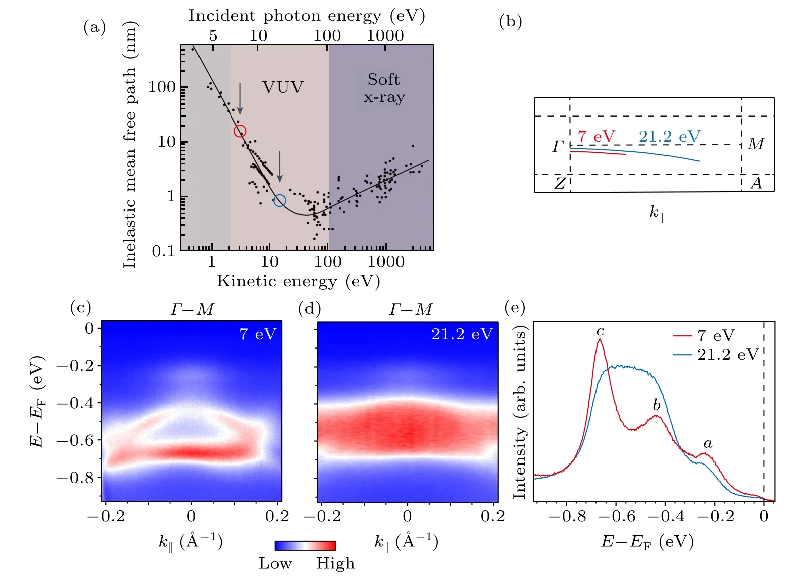
Fig.6.Comparison of the electronic structures between surface and bulk of CeTe3.(a)The inelastic mean free path of the photoelectrons as a function of kinetic energy(bottom axis)and incident photon energy(top axis).Different colors represent the separation of the energy ranges of vacuum ultraviolet(VUV)and soft x-ray light.[36](b)The moment cuts along the kz direction with photon energies of 7 eV and 21.2 eV.In order to indicate the kz positions with different photon energies,we mark them in the same BZ.(c),(d)Photoemission intensity distributions of CeTe3 along Γ–M near the Γ point with(c)7 eV photons and(d)21.2 eV photons.(e)Angle-integrated EDCs of CeTe3 with 7 eV and 21.2 eV photons over the momentum range of[-0.04 ?A-1,0.04 ?A-1].
To compare the band structures of the surface and the bulk, we conducted ARPES measurements with 7 eV and 21.2 eV photons.Figure 6(a)displays the approximate inelastic mean free path of different photon energies,from which we find the measurements performed with 7 eV photons are more bulk sensitive than those taken with 21.2 eV photons.In the photoelectric process,the electron inelastic mean free path in solids with 21.2 eV is less than 1 nm or 2 monolayers,which makes the results more easily affected by the surface, while the inelastic mean free path of electrons with a laser is about 3–5 nm or 6–20 monolayers, so the detected photoemission signals are much more bulk sensitive.To exclude the effect of band structure discrepancy at differentkzpositions,the moment cuts along thekzdirection with photon energies of 7 eV and 21.2 eV are shown in Fig.6(b).To compare directly, we mark them in the same BZ,and find that the moment cuts taken with both energies locate at approximatelykz=17.6% 2π/calongΓ–Z(M–A).Here we definekz=0 for theΓpoints.Photoemission intensity distributions alongΓ–Mdisplay apparent discrepancies in Figs.6(c)and 6(d).Three major bands can be observed in the 7 eV spectrum, which are located at binding energies of 0.24 eV,0.44 eV and 0.66 eV.These three bands can also be observed in the EDCs in Fig.6(e).With 21.2 eV photons in Fig.6(d), the band structure is quite different.Only two bands can be observed: one is narrow and locates at the lower binding energy, while the other is fairly broad and may consist of two peaks.The peak at 0.24 eV belowEFis almost at the same location with different photon energies as shown in Fig.6(e),and the broad peak with 21.2 eV photons is at a similar position with the two peaks at 0.44 eV and 0.66 eV belowEFwith 7 eV photons.To illustrate the intensity difference of the three bands in Figs.6(c)–6(e),we can refer to the photoelectric cross section as a function of photon energy in Fig.6(b).[37]With regard to the Te 5p orbital, the photoelectric cross section increases with decreasing photon energy in the range of low photon energy.This tendency is consistent with our experiment results and gives a reliable reason for the intensity differences of the two peaks at the binding energies of 0.24 eV and 0.66 eV.As for the peak at 0.44 eV belowEF,a reasonable deduction is that the hybridization between the 0.44 eV peak with other states may influence the intensity.
For CeTe3, a prototypical CDW material, our research focuses on its f-electron features and additional influencing factors such as temperature, light source energies and photon polarization.We observe that the f electrons present a dispersive quasiparticle band, indicating hybridization between the f electrons and conduction electrons.At the same time,the f electrons go through a localized to itinerant transition with changing temperature, which is common in other HF materials.[38–40]Besides, we find an energy gap in one conduction band,and the strong temperature-dependent behavior indicates that it may be related to the CDW transition.LV-and LH-polarized ARPES measurements reveal anisotropy of the orbitals with the same band, which shows different changes of intensity around theΓandMpoints, and diverse orbital symmetries with different bands displaying various changing trends.With different energies, surface and bulk band structures are fairly similar in the locations of peaks, indicating the three bands observed in the valence band structure in Figs.6(c)–6(e) are from the bulk state, which is common in some Ce-based materials.[41–43]
4.Conclusion
In summary, we have performed XRD, physical property and high-resolution ARPES measurements of the CDW f-electron compound CeTe3.Our results illustrate the comprehensive electronic structure and f-electrons features in this CDW material.We find a weakly dispersive quasiparticle band aroundEFwhich reflects the hybridization between f electrons and conduction electrons.Additionally, the localized to itinerant transition of f electrons and the energy gap probably induced by CDW are observed.We also discuss the influence of different photon energies and polarized photons on the band structure.Our findings illustrate the f-electrons properties in the CDW state of CeTe3, revealing differences between the traditional HF materials and the CDW one, and contributing to the understanding of the microscopic properties of CeTe3and other rare-earth tellurides.
Acknowledgments
Project supported by the National Natural Science Foundation of China(Grant Nos.12122409,11874330,11904334,12004349,and 11904335),the National Key Research and Development Program of China(Grants Nos.2022YFA1402201 and 2021YFA1601100), and the BL03U and BL09U ARPES beam line of Shanghai Synchrotron Radiation Facility(SSRF,China).

- Chinese Physics B的其它文章
- Robustness of community networks against cascading failures with heterogeneous redistribution strategies
- Identifying multiple influential spreaders in complex networks based on spectral graph theory
- Self-similarity of complex networks under centrality-based node removal strategy
- Percolation transitions in edge-coupled interdependent networks with directed dependency links
- Important edge identification in complex networks based on local and global features
- Free running period affected by network structures of suprachiasmatic nucleus neurons exposed to constant light