Effects of anode material on the evolution of anode plasma and characteristics of intense electron beam diode
2023-10-08 08:20:54YeHUA華葉PingWU吳平HongWAN萬紅ShuxinBAI白書欣JinyuGONG龔瑾瑜MengZHU朱夢XianchenBAI白現臣andGuangshuaiZHANG張廣帥
Plasma Science and Technology 2023年9期
Ye HUA(華葉),Ping WU(吳平),Hong WAN(萬紅),Shuxin BAI(白書欣),Jinyu GONG(龔瑾瑜),Meng ZHU(朱夢),Xianchen BAI(白現臣) and Guangshuai ZHANG(張廣帥)
1 Key Laboratory of Advanced Science and Technology on High Power Microwave,Northwest Institute of Nuclear Technology,Xi’an 710024,People’s Republic of China
2 College of Aerospace Science and Engineering,National University of Defense Technology,Changsha 410073,People’s Republic of China
Abstract In this paper,three kinds of materials including graphite,titanium(Ti) and molybdenum(Mo)are used as anodes to figure out the influence factors of anode material on the characteristics of the intense electron beam diode.The results show that the characteristics of diode are mainly determined by the cathode plasma motion under a 15 mm diode gap,in which the typical electron beam parameters are 280 kV,3.5 kA.When the diode gap is reduced to 5 mm,the voltage of the electron beam reduces to about 200 kV,and its current increases to more than 8.2 kA.It is calculated that the surface temperatures of Ti and Mo anodes are higher than their melting points.The diode plasma luminescence images show that Ti and Mo anodes produce plasmas soon after the bombardment of electron beams.Ti and Mo lines are respectively found in the plasma composition of Ti and Mo anode diodes.Surface melting traces are also observed on Ti and Mo anodes by comparing the micromorphologies before and after bombardment of the electron beam.These results suggest that the time of anode plasma generation is closely related to the anode material.Compared with graphite,metal Ti and Mo anodes are more likely to produce large amounts of plasma due to their more significant temperature rise effect.According to the moment that anode plasma begins to generate,the average expansion velocities of cathode and anode plasma are estimated by fitting the improved space-charge limited flow model.This reveals that generation and motion of the anode plasma significantly affect the characteristics of intense electron beam diode.
Keywords: anode material,anode plasma,intense electron beam,plasma expanding velocity
1.Introduction
Intense electron beam(IEB) planar diodes have important applications in high-energy radiation generation [1-4] and virtual cathode oscillators [5-10].The IEB is generated from the cold cathode by explosive electron emission process,which initiates from the surface microprotrusions of cathode under the localized high electrical field.In general,emitted electron beam energy exceeds 100 keV and current density is in the order of kA cm-2.When the anode is bombarded by the IEB,anode plasma could appear under certain conditions[6,7,9,11-14].The developments of cathode and anode plasmas may result in impedance collapse [9,12,13],which seriously affects the normal operation of diode.Therefore,it is important to reduce the plasma propagation velocity in the planar diode.Previous studies of planar diodes have focusedon improving cathode materials to reduce the rate of cathode plasma expansion,while less attention has been paid to anode plasma.
The anode plasma could be generated by either melting and subsequent evaporation of the anode material or by electron stimulated desorption of the contaminants on the anode surface[12,15],depending on the temperature and gas adsorption state of the anode surface after the bombardment of IEB.This indicates that time is needed for producing anode plasma,especially when the anode material melts to produce a large amount of plasmas.In fact,the surface temperature of the anode is difficult to be directly measured due to extremely fast temperature rises and cooling,about a few to dozens of nanoseconds.
Considering the difficulty of transient temperature measurement,some researches paid more attention to electron incident depth and resistance to thermal destruction of the anode materials [7,10,16,17].They simulated the process that IEBs bombard on different simple materials,the results show that the accelerating voltage and the material properties,such as atomic number,atomic mass,and density of the material,affect the depth-energy relationship[7,10].Then the surface temperature rise can be calculated from the depthenergy relationship,current density,density and heat capacity of the material if diffusion,convection and heat radiation are neglected [7,10,16,17].
Graphite,titanium(Ti) and molybdenum(Mo) have different in atomic numbers,density,heat capacities,and melting points[10,16].This results in different performances in heating effects of IEB to the anode material as well as diode characteristics [10,16,17].To clearly figure out the influence of anode materials on the characteristics of the diode,in this work,three simple materials are respectively used as anodes in an IEB diode.Two kinds of IEBs,different in electron energy and energy density,are severally collected by graphite,Ti and Mo anodes.Firstly,the experimental device and diagnostic equipment used are briefly introduced.The characteristics of the diode are displayed and analyzed according to the evolution of plasma,and then the cathode and anode plasma expanding velocities are calculated based on the revision of the bipolar flow model.
2.Experimental setup
The experimental configuration is shown in figure 1.A pulsed power source provides a high-voltage pulse,with an amplitude of 200-350 kV.The pulse passes through the spark gap switch and spiral transmission line to the diode,which consists of an annular graphite cathode(with an outer diameter of 39 mm and a blade width of 0.5 mm) and a planar anode.The anode consists of a target and a stainless steel planar base with a diameter of 150 mm.The target with an outer diameter of 57 mm is embedded in the groove of the base.The graphite cathode and each anode are pretreated by ultrasonic cleaning and vacuum baking at 200 °C for 2 h to remove absorbed contaminants and water vapor before being assembled.The diode operates at a base pressure under 5×10⁻²Pa with a molecular pump providing the vacuum.The diode voltage and current are measured by a resistance divider and Rogowski coil,respectively.In addition,a high speed frame camera(HSFC) is applied to record the diode plasma luminescent images through an optical window on the side of the diode.The HSFC is triggered by a transistor-transistor logic signal,which is switched from the high-voltage pulse by a signal processor.The high-voltage pulse is identical in shape to the pulse arrived at the diode,but differs in time.The additional spiral transmission line is added to realize the accurate synchronization between the exposure time of camera and the luminescence process of diode plasmas.Also,a fiber optical integral spectrometer is used for the measurement of diode plasma optical emission spectrum through the optical window.In order to avoid the reflection light,the inner surface of the vacuum chamber has been covered by some low-reflectivity material [18].To obtain two kinds of IEBs with different electron energies and energy densities,the anode-cathode(A-K) gap is fixed at 15 mm and 5 mm,respectively.The microscopic morphologies of the anodes are observed by a scanning electron microscope.
3.Results and discussion
3.1.A-K gap of 15 mm
The diode voltage and current waveforms for 15 mm A-K gap are shown in figures 2.It can be found that the diode voltage and current behaviors are similar for all kinds of anodes.The diode line voltage and current for different anodes are all~280 kV and ~3.5 kA,respectively.
The diode impedance and perveance curves derived from the experimental voltage and current corresponding to graphite anode at A-K gap of 15 mm are shown in figure 3.One can observe that the diode impedance is always higher than zero in the whole duration of the pulse,and it remains slightly variable between 40 ns and 140 ns.The diode perveancePdiode,which mainly reflects the diode characteristics resulted from the changes of cathode emission area and A-K gap,is related to diode currentImeaand voltageUd,as shown in equation(1)[19].The perveance curves could be divided into three stages,and they are all in connection with the evolutionof diode plasma.The first stage is from the start of the electron emission to ~20 ns.The diode perveance increases linearly in this stage,which corresponds with the increase of cathode effective emission area resulted from radial expansion and combination of cathode local plasma spots.The second stage starts from ~20 ns and ends at ~130 ns.In this stage,the perveance increases slowly,which may be in accordance with the axial expansion of cathode plasma.The third stage is the decrease of perveance,which may be due to the reflection of the voltage wave.
To further determine whether the anode plasma is produced,the HSFC was applied to record the diode plasma luminescent images at different moments.Figure 4 shows the typical diode plasma luminescence images in different periods for the graphite anode.The graphite annular cathodes are on the left,and anodes are all on the right.It can be observed that cathode plasma spots appear first,and then the number and the light intensity of cathode plasma spots increase gradually,along with the axial expansion.There is no anode plasma spot in the duration from 0 to 192 ns,which includes the whole pulse of the diode current,as shown in figure 2.
3.2.A-K gap of 5 mm
The diode voltage and current waveforms for a 5 mm A-K gap are shown in figure 5.It can be found that the rise edges of diode voltage curves are similar for all of the anodes,but the drop edges are different,resulting in the difference of pulse durations of diode voltages.The diode current curves are almost identical for all of the anodes at the beginning stage of explosive electron emission,which corresponds to the duration from 0 to ~60 ns.However,the middle segments from ~60 to ~170 ns are distinct in both shape and size for different anodes.In addition,the diode line voltage is ~200 kV; however,the diode line currents for the graphite,Ti and Mo anodes are ~8.2 kA,~11.1 kA and~11.7 kA,respectively.Furthermore,the amplitude of diode voltage at 15 mm A-K gap is obviously higher than that of 5 mm A-K gap,which suggests the larger kinetic energy of electron beam in diode with 15 mm A-K gap.
According to the diode voltage and current waveforms displayed in figures 2 and 5,the beam energy collected by graphite anodes under different A-K gaps can be calculated,as depicted in figure 6.It can be easily observed that the energies of one pulsed electron beam collected by graphite anodes under 15 mm and 5 mm A-K gaps are ~103 J and~150 J,respectively.Besides,the area of the anode surface bombarded by the cathode electron beam increases with the A-K gap for no limitation of external magnetic field.In consequence,the energy density of electron beam arriving at the anode surface in diode with 15 mm A-K gap is much lower than that in the diode with a 5 mm A-K gap.The temperature rise of the anode surface is positively correlated with the energy density of the electron beam acting on it[7,10].Therefore,the surface temperature of the anode under 5 mm A-K gap is higher than that of the 15 mm A-K gap.
The energy depositions of a 200 keV electron beam in graphite,Ti and Mo are calculated by the Monte Carlo N-particle transport code,Version 5.In calculations,the target with a vertical incident thickness of 0.3 cm is set,and the target is divided into 300 grid elements with thicknesses of 0.001 cm.The physical property parameters of the materials listed in table 1 are used in the calculation.
It is suspected that the melting of the coating is related to the temperature increase caused by electron beam energy deposition.Neglecting diffusion,convection,and for the moment also heat radiation enables estimating the overall temperature increase by incorporating the depth-energy relation,as shown in figure 7(a).Under the condition of adiabatic approximation and the assumption that the heat capacity and density of the material remain constant during the irradiation,the temperature rise of celliis estimated as:
Here,Cis the heat capacity of the material,ρis the density of the material,Sis the area of the electron beam bombarded on the target,dis the thickness of the celli,eis electron charge,Eiis the deposited energy in the celli,Neis the number of incident electrons,Ibis the current of the electron beam,t0andt1are thestarting and ending moments of the pulsed electron beam,respectively.According to figure 5,the starting and ending moments of the pulsed electron beam are about 0 ns and 180 ns,respectively.The diode current corresponding to the graphite anode in figure 5 is taken as the electron beam currentIb,thenThe area of the electron beam bombarded on the targetScan be measured by damage marks on the target,which is calculated to be about 7.01 cm2.The values of density and heat capacity are exhibited in table 1.Then the temperature rise of the three materials can be calculated by equation(2),as shown in figure 7(b).It is observed that the supreme temperature rises of graphite,Ti and Mo are separately about 1233 °C,1746 °C,and 3235 °C,respectively.The supreme temperature rise in the graphite is less than its melting points,while the supreme temperature rises in the Ti and Mo are higher than their melting points shown in table 1.Therefore,it can be inferred that Ti and Mo anodes may produce a large amount of plasmas for their melting in diode with 5 mm A-K gap.
The diode impedance and perveance curves derived from the experimental voltage and current corresponding to different anodes for a 5 mm A-K gap are shown in figure 8(a)and(b),respectively.From the start of the electron emission to ~60 ns,the diode impedance and the perveance corresponding to the three anodes basically change synchronously.In the duration from ~60 to 180 ns,the diode impedance slowly drops to zero,and then diode impedances of Ti and Mo anodes increase,corresponding to the reversing of voltage and current,as shown in figure 5.At this time,the diode perveance increases speedily,but there is a significant difference in the moments when the perveance begins to increase rapidly.The results indicate that the gaps of diodes with the three anodes are all closed in the later stage of the pulse.In general,the closure of diode is attributed to the expansion of plasma produced by cathode or/and anode.The plasma expansion speed of graphite cathode is about 2 cm/μs(according to 2 ± 0.5 cm/μs in [20],2.4 cm/μs in [21],and 1.8 cm/μs in [22]).If the anode plasma is ignored,the decrease of the A-K gap in the whole duration(~180 ns)can be calculated to be about 3.6 mm,which is less than the initial A-K gap(5 mm) and will not result in a gap closure.Consequently,it is suspected that the anode plasma was generated during this process.The difference of impedance for diodes with different anodes in size in the later stage may be due to the differences in time of generation and expanding velocities of the anode plasmas produced by different anodes.
The diode plasma luminescence images at 5 mm for the graphite,Ti and Mo anodes are displayed in figure 9.It can be found that the anode plasma generates and expands axially over time.The anode plasma generated by the graphite anode is the latest and the area of the anode plasma spots is the smallest.However,the anode plasmas generated by the Ti and Mo anodes result in the larger area of the anode plasma spotscompared with that generated by the graphite anode at the same moment.The moments that anode plasmas begin to generate for the graphite,Ti and Mo anodes are during the period of 114-154 ns,3-13 ns and 4-14 ns,respectively.
Table 1.Some physical parameters of graphite,Ti and Mo.
Figure 10 displays the diode plasma optical emission spectra at 5 mm A-K gap for various anodes.According to the atom spectra database lines data of National Institute of Standards and Technology(NIST) [23],most of the lines in the spectra are identified.There are a lot of Carbon(C),Hydrogen(H) and Sodium(Na) lines in the diode with each anode.Meanwhile,Ti or Mo lines are respectively detected in the diode with Ti anode or Mo anode,which indicates that Ti anode and Mo anode have produced anode plasma by melting and subsequent evaporation of themselves.The H and Na particles appeared in the diode are probably generated by the adsorbed gas and containments.Nevertheless,even though there are many C lines in diode with the graphite anode,it is not clear whether or not the graphite anode produced anode plasma when the cathode is also graphite.
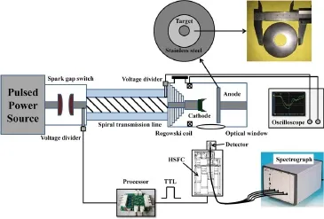
Figure 1.Schematic diagram of the experimental setup.
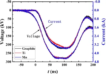
Figure 2.Diode voltage and current waveforms for diodes with different anodes at the A-K gap of 15 mm.
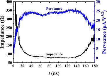
Figure 3.The typical diode impedance and perveance curves at A-K gap of 15 mm.
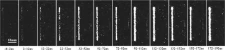
Figure 4.Typical diode plasma luminescence images in different periods for graphite anode at A-K gap of 15 mm.
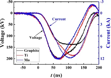
Figure 5.Diode voltage and current waveforms for diodes with different anodes A-K gap of 5 mm.
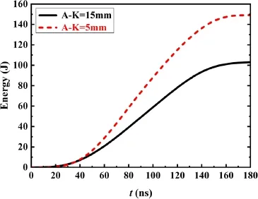
Figure 6.The beam energy collected by graphite anodes under 15 mm(a) and 5 mm(b) A-K gaps.
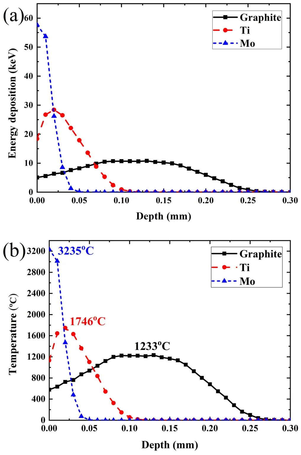
Figure 7.Energy deposition distribution curves of a 200 keV electron in graphite,Ti and Mo(a) and the temperature rise caused by the heating of electron beam energy deposition(b).
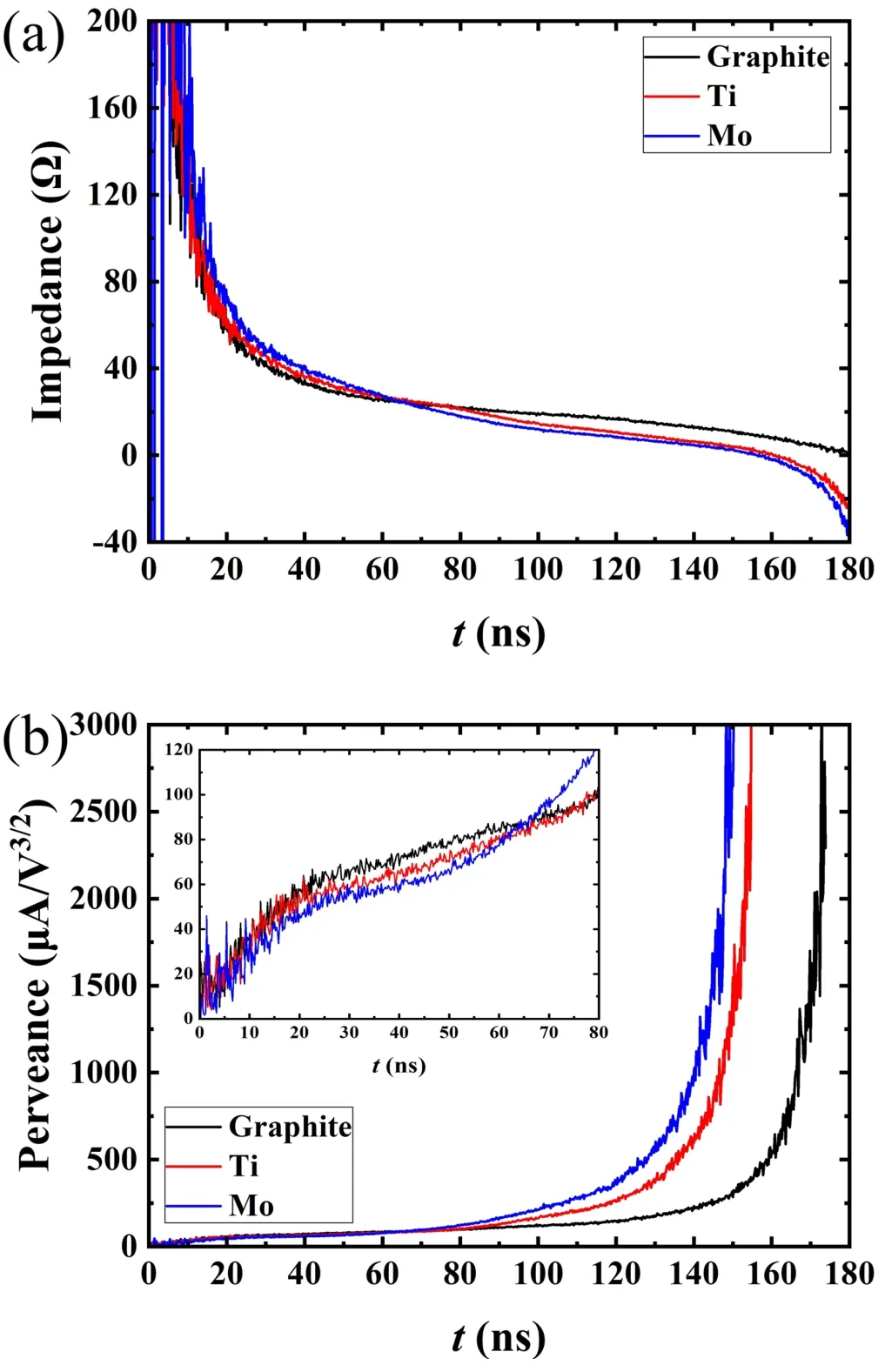
Figure 8.Diode impedance and perveance curves for diodes with different anodes at an A-K gap of 5 mm.

Figure 9.Diode plasma luminescence images in different periods for graphite anode(a),Ti anode(b)and Mo anode(c)at A-K gap of 5 mm.On the left is cathode plasma and on the right is anode plasma.
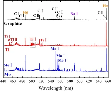
Figure 10.Diode plasma optical emission spectra for various anodes at the A-K gap of 5 mm.
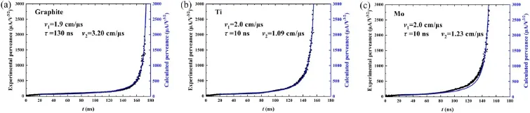
Figure 12.Temporal dependence of the experimental and calculated perveances for diodes with different anodes:(a)graphite,(b)Ti,(c)Mo.
The microscopic morphologies of the three anodes before and after several shots of IEBs are also observed,as shown in figure 11.One can see from figures 11(a) and(b) that the particles fall off from the graphite surface after several pulses,however,there is no trace of melting.The reason for this phenomenon can be explained by the fact that the carbon on the graphite surface will oxidize slightly with the released gas as the temperature increases due to the surface and internal porosity of the graphite [24,25].The melting traces havebeen observed on the surfaces of Ti and Mo targets after the bombardments of IEBs,which can support the inference from figures 7 and 10.
To sum up,plasma luminescence images show that the plasmas on Ti and Mo anodes are formed quickly and in large quantities.Plasma spectrum shows that the composition of plasma contains metal atoms or ions,which suggests that metallic vapors contribute to the formation of plasma.Usually,there is adsorption gas on the surface of the material.When the temperature rises to its melting point,the surface of the material forms a vapor layer.The anode plasma could be generated by either melting and subsequent evaporation of the anode material or by electron stimulated outgassing and desorption of the contaminants on the anode surface[12,15].When a pulsed electron beam acts on the surface of the material,surface temperature of the material increases gradually,resulting in the increase of the outgassing.The vapor of the material itself will be produced continuously when the temperature exceeds the melting point of the material.According to the results above,the formation process of anode plasma in one pulse duration is inferred as follows.At the beginning of electron beam action,the anode surface adsorption and dissolved gas are continuously released,and the gases are ionized and the anode plasma is formed.With the continuous action of the electron beam and plasma,the surface temperature of the anode increases.When the surface temperature of the anode increases to its melting point,the vapor produced by self-gasification of the material will also be ionized to form plasma,which is also an important part of the anode plasma.The generations and concentrations of released gas and material vapor are positively related tosurface temperature of the anode.Compared with Ti and Mo anodes,the formation time of plasma on the surface of the graphite anode occurs later and produces less.The main reason for this is that the surface temperature rise of the graphite anode is much lower than those of Ti and Mo anodes under the action of electron beam,as shown in figure 7(b).
The expansion velocity of plasma is also a key factor affecting the characteristics of IEB diode.When the anode plasma can be ignored,the diode perveance can be given by the one dimensional(1D) Child-Langmuir law,as shown in equation(3) [9],
whereeandmeare the charge and mass of electron,ε0is the absolute permittivity of vacuum,Ud(t) is the diode voltage,d0is the A-K gap,v1is the average speed of cathode plasma axial expansion,andSis the emission area of the cathode.What needs illustrating is that the radial expansion of the cathode plasma can be ignored after ~20 ns,at which point,the cathode can be considered as being completely covered by plasma and the cathode emission area scarcely changes.
However,if the anode plasma is generated and forms a bipolar electron flow,the model for the bipolar space-charge limited flow in the presence of the plasma expanding from the cathode and anode surfaces can be expressed by equation(4)[12],
wherev2is the average speed of the anode plasma axial expansion.In fact,it could be some time delay in the anode plasma formation with respect to the cathode plasma generation,as shown in figure 5.In this case,equation(4)should be modified with respect to the value of [d0-(v1+v2)t] by[d0-v1t-v2(t-τ)],as shown in equation(5).Here,τis the time that the anode plasma begins to generate.
Therefore,the perveance expression for the electron bipolar flow of the diode can be described by
In addition,a perveance expression for the cathode surface must also include the effect of electron flow from the cathode circumferential edge.Edge effects in finite area diodes may significantly increase the value of the space-charge limited current relative to the prediction of the 1D Child-Langmuir law [26].Contribution due to edge can be accounted for by using Langmuir-Compton equation for cylindrically symmetric space-charge limited electron flow,as shown in equation(7) [26].Edge effects in finite area diodes may significantly increase the value of space-charge limited current relative to the prediction of the 1D Child-Langmuir law[25].
whereα=ln(d0/v1t)-0.4[ln(d0/v1t)]2+0.0917[ln(d0/v1t)]3-0.0142[ln(d0/v1t)]4+...,r0is the cathode radius.
The perveance of the total bipolar electron flow from the cathode edge and face is equal to the sum of two components.Thus,the diode perveance in the generalized form can be expressed as
Considering the discrepancy of time delay in the anode plasma formation with respect to the cathode plasma generation for different anode materials,the calculation of diode perveance should be divided into two parts according to the value ofτ
Thus,the cathode emission area,the expansion velocities of cathode and anode plasma,and the time that the anode plasma begins to generate are the only parameters that can affect the diode perveance.
Based on equation(9)and the moment that anode plasma begins to generate obtained from figure 9,the experimental perveances for diodes with different anodes are fitted,as shown in figure 12.The best fit for the theoretical model was obtained assuming optimal parameters,which are displayed in figure 12.The results indicate that the average speed of cathode plasma axial expansion is independent of anodes for almost the samev1,however,τandv2are closely associated with the anode material.τis later andv2is faster for diode with graphite anode compared with the diodes with Ti anode and Mo anode.Also,the plasma axially expanding average velocities of Ti and Mo are distinct.It is well known that the plasma expansion velocity is inversely proportional to the particle mass[27],which means that the heavier the particles in the plasma,the lower expanding velocity of the plasma.According to the composition of plasma obtained from plasma optical emission spectra,only the lighter C,H and Na elements are detected in the plasma for diode with graphite anode,whereas Ti and Mo atoms or/and ions with greater mass exist in the plasmas for diodes with Ti anode and Mo anode.
4.Conclusions
The IEB diodes with annular graphite cathodes and three different planar anodes have been investigated under A-K gaps of 15 mm and 5 mm.It is found that the characteristics of diodes with graphite,Ti and Mo anodes are not significantly different when the A-K gap is 15 mm,while visible differences are observed at the A-K gap of 5 mm,reflecting in the diode current waveform and amplitude.Analyses from various means suggest that the main reason is the difference of anode materials properties and the resulting temperature rise effect after IEB bombardment.Firstly,the surface temperatures of Ti and Mo anodes are higher than their melting points when a 200 kV,8.2 kA and 120 ns electron beam bombards them,which are confirmed by the calculation of temperature rise and microscopic traces of surface melting.Secondly,Ti lines and Mo lines are respectively found in the plasma composition of Ti and Mo anode diodes.Thirdly,a lot of plasmas have been observed on the surface of Ti and Mo anodes soon after the bombardment of electron beams,while the amount of plasma on the surface of the graphite anode is small and the formation time is relatively late.Based on this phenomenon,the average expansion velocities of cathode and anode plasma are estimated by fitting the improved spacecharge limited flow model.Therefore,it can be concluded that the main factors affecting the characteristics of IEB diode are the generation and motion of plasma,which are closely related to energy density of IEB and the anode materials.
Acknowledgments
The authors would like to thank Dr D Cai,Dr H T Wang,Dr X L Sun and Mr L Luo for their help in experiments.
 Plasma Science and Technology2023年9期
- Plasma Science and Technology的其它文章
- Plasma Science and Technology
- The magnetic field design of a solenoid for the cold-cathode Penning ion source of a miniature neutron tube
- Research on the energy consumption mechanism and characteristics of the gallium indium tin liquid metal arcing process
- Chemical and physical studies of metallic alloy-based old Indian coins with LIBS coupled with multivariate analysis
- Simulation of DC glow discharge plasma with free-moving dust particles in the radial direction
- Experimental studies on the propagation of whistler-mode waves in a magnetized plasma structure with a non-uniform density