Enhanced and controllable reflected group delay based on Tamm surface plasmons with Dirac semimetals
2023-09-05 08:48:04QiwenZheng鄭棋文WenguangLu盧文廣JiaqingXu胥加青YunyangYe葉云洋XinminZhao趙新民andLeyongJiang蔣樂勇
Chinese Physics B 2023年7期
Qiwen Zheng(鄭棋文), Wenguang Lu(盧文廣), Jiaqing Xu(胥加青),Yunyang Ye(葉云洋),?, Xinmin Zhao(趙新民),?, and Leyong Jiang(蔣樂勇)
1School of Physics and Electronics,Hunan Normal University,Changsha 410081,China
2School of Intelligent Manufacturing and Electronic Engineering,Wenzhou University of Technology,Wenzhou 325035,China
3School of Electronic Science and Engineering,National University of Defense Technology,Changsha 410073,China
Keywords: group delay,Tamm plasmons,Dirac semimetals
1.Introduction
Group delay generally indicates the speed of the phase change relative to angular frequency when an electromagnetic wave pulse passes through a medium or structure.It is a typical optical phenomenon in the transmission of optical pulses.[1,2]Since the delay time of reflected and transmitted pulses can be manipulated from subluminal to superluminal by controlling the dispersive properties of the medium,[3]it is clear that research on group delay plays an important role in many fields, such as optical communications,[4,5]signal modulation,[6]delay lines,[7]optical storage[8]and fiber laser systems.[9]Therefore,researchers have investigated group delay enhancement and regulation in various structures.For example,the delay phenomenon in an analog circuit model,[10,11]photonic crystal (PC) structure[12]and Fabry–Perot cavity structures[13]has attracted extensive attention.In addition,Wang and Zhu studied the phenomenon of reflected optical pulse group delay of a weakly absorbing dielectric slab, and obtained a negative group delay of?4 ps.[14]Yaoet al.studied the tunable group delay in a Fabry–Perot cavity, and regulated the negative group delay by adjusting the polarization azimuthal angle of the incident pulse.[15]Recently, Xuet al.realized microsecond level reflected and transmitted group delay based on excitation of a topological edge state in a PC heterostructure.[16]Although researchers have studied many delay phenomena based on various structures and proposed many methods to enhance group delay,it is still a challenge to study delay approaches and schemes with large group delay.The exploration of micro-nanostructures with large group delay combined with new materials has attracted much attention.Graphene, a two-dimensional (2D) material, can be taken as a representative example; it has obvious advantages not only in electrically controllable optical phenomena and devices,2D optics and other fields,[17–19]but also in realizing enhanced delay due to its excellent photoelectric characteristics.[20,21]Researchers have studied many ways to enhance and manipulate the reflected group delay of optical pulses in graphene-based micro-nanostructures.For example, Wanget al.studied the regulation characteristics of reflected group delay in the mechanisms of both resonances and the excitations of surface plasmon resonances in graphene-based layered systems.[22]Xuet al.studied the tunable bistable reflected group delay based on a modified Otto configuration with the insertion of monolayer graphene and a nonlinear substrate.[23]It is not difficult to see that the enhancement and regulation approach to group delay based on 2D materials will be a feasible direction to realize practical delay devices, and this still represents the direction of study of optical delay,with large group delay,easier adjustment and a simple structure.
In terms of mechanism, the optical Tamm state (OTS),as a lossless interface mode localized at the boundary of two different periodic dielectric structures, also has advantages in the field of enhanced group delay.[24]Compared with surface plasmons, the OTS does not need a specific incident angle to achieve wave vector matching, and can even be excited at vertical incidence.[25]At present, the structures which excite the OTS are mainly one-dimensional(1D)crystal heterostructures[26]and metal-distributed Bragg reflector(DBR)structures.[27]In addition,when the OTS is excited,it will be accompanied by a strong local field enhancement effect,and the OTS corresponds to the reflected resonance peak in the photonic band gap range.[28]These characteristics of the OTS mean that it has been widely studied in relation to absorption characteristics,[29]the nonlinear Kerr effect[30]and optical sensors.[31]The excitation of an OTS is often accompanied by phase mutation,thus creating conditions for the realization of large delay.Therefore, this provides an effective way to design optical devices with large group delay.In recent years,bulk Dirac semimetals(BDSs)have attracted attention.Such materials can be roughly regarded as‘3D graphene’,because BDSs are similar to graphene in many ways and their Fermi energy can be adjusted by chemical doping and changing the bias voltage,[32]so as to change the permittivity.[33,34]At present, BDSs have been applied in the fields of light absorbers and optical sensors.For example,Liuet al.proposed a terahertz tunable narrowband absorber based on a BDS which realizes dynamic regulation of the absorption frequency by adjusting the Fermi energy.[35]Yeet al.proposed a highsensitivity tunable terahertz sensor based on a BDS to solve the problem of low figure of merit (FOM); they verified that the FOM of the sensor reached 6001.[36]At the same time,BDSs show a metal response at frequencies lower than the Fermi energy and a dielectric response at frequencies higher than the Fermi energy.[37]Therefore, adding a BDS to a specific optical structure to excite OTS is a way to obtain adjustable large group delay.The conductivity characteristics of a BDS are similar to those of graphene, and the advantages in design of delay devices can therefore be retained.However,BDSs have a certain thickness, so requirements for preparation, transfer and processing are lower than those for graphene.In order to control the reflected group delay, a multilayer composite structure composed of a BDS and DBR is proposed in this paper.The OTS is excited by the BDS and 1D PC structure,combined with the optimization of the structural parameters to obtain a large positive and negative group delay.We believe that tunable and large group delay based on a BDS composite structure can find potential applications in photoelectric detection,sensing,communication and other fields.
2.Theoretical model and method
We consider a composite structure composed of a BDS and 1D PC to excite the OTS.The spacer layer is placed between the BDS and the PC,as shown in Fig 1.The 1D PC is composed ofTalternating cycles of dielectric layer A and dielectric layer B.We set the refractive index of dielectric layer A with thicknessdAasnA=1.47 and that of dielectric layer B with thicknessdBasnB=1.9.Their refractive indices in the terahertz band can be obtained from polymethylpentene and SiO2,respectively.This simple multilayer structure based on actual material parameters is not difficult to realize with current preparation processes.This also lays a foundation for the experimental implementation based on this scheme.There are also many schemes for the experimental measurement of group delay.[38,39]In the following calculation, we set the periodT=20, the central wavelength isλc=60 μm and the thickness of media A and B aredA=λc/(4nA) anddB=λc/(4nB).In order to simplify the calculation, only the case of TE polarization is considered.When low-temperature conditionsT ?EFare met, the conductivity of the BDS can be approximately expressed as[37]
wheregrepresents the degeneracy factor.Its different values correspond to different specific BDS materials.[40]After calculation and comparison, we found that a BDS corresponding tog= 40 (AlCuFe quasicrystal[41]) meets most of our demands for large group delay.Also in these equationsfrepresents the frequency, Fermi velocityvFis 106m·s?1,EFis Fermi energy, the Fermi momentum iskF=EF/ˉhvF, ˉhis the reduced Planck constant,?(f)=2πˉhf/EF+iˉhτ?1/EF,whereτ=μEF/v2Fis the electron relaxation time,μis the carrier mobility andεc=Ec/EF, whereEcis the cut-off energy.Once this energy is exceeded,the Dirac spectrum will no longer be linear.Based on the above formula,the relationship between the dielectric constant of the BDS and its conductivity can be expressed as
whereεb=1 is the effective background dielectric constant andε0is the permittivity of a vacuum.It can be seen from the above expression that the Fermi energy plays a key role in characterizing the conductivity of the BDS, and the Fermi energyEFcan be controlled by applying an external voltage,which provides an effective way to regulate the reflected group delay of the composite structure.

Fig.1.Schematic diagram of a 1D PC structure containing a BDS.
In order to calculate the reflected group delay of the structure in Fig.1, we use the transfer matrix method to calculate the reflection coefficient of the BDS–DBR structure.The interaction between a medium and light waves can be completely determined by the characteristic matrix of the medium layer.Based on the boundary conditions, the characteristic matrixMjof a single-layer medium can be obtained from
whereηj=Kj/εj.For a structure with a multilayer medium,the characteristic matrix of the multilayer mediumMtotalcan be obtained by multiplying the characteristic matrix of each layer
Based on the characteristic matrix of the whole composite structure, the matrixMfor the whole structure can be obtained as follows:
By defining the optical admittanceY=C/Bof the structure,the reflection coefficient of the structure can be obtained by
Based on the transfer matrix method, on the condition of a narrow spectrum Gaussian pulse,it is easy to calculate the reflected group delay as follows:
In the following calculations, we set as the initial conditions a Fermi energyEF=0.3 eV, relaxation timeτ=0.9 ps and thickness of the BDS layerdBDS=20 nm;the dielectric constant and thickness of the spacer layer are consistent with those of dielectric layer B.
3.Results and discussions
First we discuss the reflectance of a 1D PC composite structure with or without a BDS, 1D PC and separate BDS layer,as shown in Fig.2.It is obvious from Fig.2 that when there is no BDS the reflectance of the 1D PC is almost 1 in a certain frequency range due to the band gap, which indicates that the PC has a blocking effect on the photons in this frequency band, forming the photonic band gap.The addition of a BDS makes the curve of reflectance show an obviously reflected dip (nearf=4.84 THz) in the photonic band gap.Whenf=4.84 THz is obtained from Fig.2,the reflection coefficientrBDSof an electromagnetic wave incident from the spacer layer to the BDS and the reflection coefficientrDBRof an electromagnetic wave incident from the spacer layer to the PC can be found to satisfyrBDSrDBRexp(2iδ)≈1,Arg(rBDSrDBRexp(2iδ))≈0.These expressions mean that the OTS will be excited.[25]It should be noted that the structure of Fig.1 can also be seen as an optical Fabry–Perot cavity composed of a BDS and DBR.Therefore, the reflected peak in Fig.2 is also very similar to excitation of the Fabry–Perot mode.However, the numerical calculation shows that the thickness of the spacer layer does not meet the minimum thickness required for the Fabry–Perot mode.This further verifies that the reflected peak in Fig.2 is caused by OTS excitation: the excitation of OTS leads to dramatic changes in the reflected phase, creating conditions for achieving large group delay.
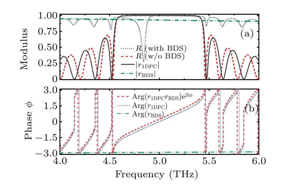
Fig.2.(a)Dependence of the reflection spectra on frequency for different structures.(b)Dependence of the reflected phase on frequency.
Next,we discuss the influence of the Fermi energy of the BDS on the reflected group delay.Figure 3 shows the dependence between the reflected phase and reflected group delay on frequency of the composite structure for different Fermi energies.According to formulae(1)–(3),when the Fermi energy changes,the conductivity of the BDS also changes,which further affects the permittivity of the BDS and finally leads to different group delays.Therefore, by applying an external voltage to change the Fermi energy of the BDS we can dynamically adjust the value of reflected group delay.When the Fermi energy increases,the position of resonant frequency shifts to the right,and the curve of the reflected phase becomes steep, as shown in Fig.3(a).The change in the phase is directly reflected in the value of the group delay.As shown in Fig.3(b),when the Fermi energy is 0.25 eV a reflected group delay of about?11.75 ps can be obtained.Continuing to increase the Fermi energy can help us obtain a greater negative group delay.For example, when the Fermi level is 0.4 eV,the reflected group delay is about?65.7 ps.At the same time,the resonance frequency of the OTS also moves towards a higher frequency with increase in the Fermi energy.These phenomena show that the reflected group delay of the composite structure is very sensitive to changes in the Fermi energy.The Fermi energy plays an important role in determining the value of group delay.In practical manipulations we can adjust the Fermi energy by adding electrodes between the BDS and the substrate.[42]This electronic control characteristic of the reflected group delay provides a way to design tunable group delay devices.For the convenience of discussion, we set the Fermi energy as 0.4 eV in the next calculation.

Fig.3.Dependence of the(a)reflected phase and the(b)reflected group delay on frequency of composite structures for different Fermi energies.
Apart from the dynamic manipulation of group delay by Fermi energy,it is known from formulae(1)–(3)that the electron relaxation time of a BDS also has a significant impact on its conductivity.According to calculations by the transfer matrix method,the reflected group delay will also be very sensitive to the electron relaxation time.This characteristic provides a new way to regulate the reflected group delay.With the Fermi energy taking the fixed value set previously we plotted the dependence of the reflected group delay and the reflected phase on frequency for different electron relaxation times, as shown in Fig.4.Compared with the influence of Fermi energy on the reflected phase and the reflected group delay,the influence of electron relaxation time on the reflected group delay is mainly shown by the value of the peak of group delay,and the resonance frequency of the reflected phase and the reflected group delay will not be changed.Further,we find that changing the electron relaxation time of the BDS can change the monotonicity of the reflected phase,thus changing the positive and negative phases of the reflected group delay.Excitation of the OTS will make the reflected phase an obvious monotonic decreasing or monotonic increasing process.Referring to the calculation of reflected group delay,this monotonous process of the reflected phase corresponds to a specific group delay peak.This regulation characteristic provides a way to convert positive and negative reflected group delay.However,it should be noted that, for a certain structure, once the Fermi energy takes a fixed value and the structure is determined it will become difficult to change the relaxation time.However,for the BDS–DBR composite structure, according to the expression for electron relaxation time of the BDS,the relaxation time is regulated by the Fermi energy,so the relaxation time can also be regulated by adjusting the external voltage.

Fig.4.Dependence of(a)the reflected phase and(b)the reflected group delay on frequency for different relaxation times.
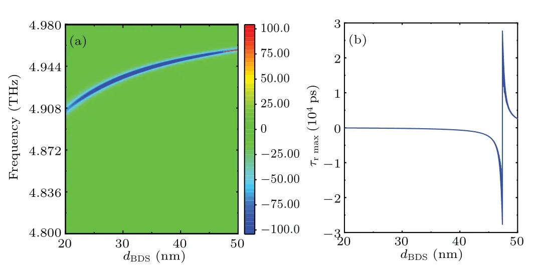
Fig.5.(a) Reflected group delay of the system as a function of the thickness of the BDS and frequency.(b)Dependences of the maximum group delay value on the thickness of BDS.
Next, we discuss the effect of structural parameters of the BDS–DBR composite structure on reflected group delay.These conclusions will provide key references for the design of regulable group delay devices.Figure 5 shows the group delay according to the thickness of the BDS for different frequencies and the dependence of the maximum group delay value on the thickness of the BDS.It is not difficult to find from Fig.3 or Fig.4 that excitation of the OTS will make the reflected phase an obvious monotonic decreasing or monotonic increasing process.Referring to the formula for calculating reflected group delay, this monotonous process of the reflected phase corresponds to the specific group delay peak.The material parameters or structural parameters of the scheme have similar effects on group delay.As shown in Fig.5, change in BDS thickness essentially regulates its permittivity.With increase in BDS thickness,the slope of the monotonically decreasing reflected phase at the resonance frequency gradually decreases and tends to negative infinity.In terms of group delay,this trend is reflected as a negative group delay with an increasing absolute value.As the BDS thickness continues to increase,the reflected phase will jump from negative to positive due to the jump from negative infinity to positive infinity,resulting in a sudden jump from a negative group delay peak to a positive group delay peak, which is exactly what is seen in Fig.5(b).After the scheme has relatively optimized the initial parameters,the maximum group delay caused by surface waves shows a similar hyperbolic trend with change in thickness of the BDS layer.From this trend,we can easily estimate the thickness of the BDS layer that corresponds to a large reflection group delay.
4.Conclusions
In conclusion, we have theoretically studied the regulation of reflected group delay when the OTS is excited in a BDS–DBR structure.The numerical calculation results show that large group delay in this configuration can be realized due to the excitation of the OTS at a BDS–dielectric interface.The regulation of group delay mainly depends on the conductivity characteristics of the BDS.We also found that the reflected group delay is very sensitive to BDS material and structural parameters.These results provide a feasible way to control the delay characteristics of terahertz pulses.We believe that this scheme will be helpful for the design and preparation of controllable group delay devices.
Acknowledgements
Project supported by the Scientific research project of Zhejiang Provincial Department of Education (Grant No.Y202250547),the Scientific Research Project of Wenzhou University of Technology(Grant No.ky202205),and the Hunan Provincial Natural Science Foundation of China (Grant No.2022JJ30394).

- Chinese Physics B的其它文章
- First-principles calculations of high pressure and temperature properties of Fe7C3
- Monte Carlo calculation of the exposure of Chinese female astronauts to earth’s trapped radiation on board the Chinese Space Station
- Optimization of communication topology for persistent formation in case of communication faults
- Energy conversion materials for the space solar power station
- Stability of connected and automated vehicles platoon considering communications failures
- Lightweight and highly robust memristor-based hybrid neural networks for electroencephalogram signal processing