High performance SiC trench-type MOSFET with an integrated MOS-channel diode
2023-03-13 09:20:18JieWei魏杰QinfengJiang姜欽峰XiaorongLuo羅小蓉JunyueHuang黃俊岳
Chinese Physics B 2023年2期
Jie Wei(魏杰) Qinfeng Jiang(姜欽峰) Xiaorong Luo(羅小蓉) Junyue Huang(黃俊岳)
Kemeng Yang(楊可萌)1, Zhen Ma(馬臻)1, Jian Fang(方健)1, and Fei Yang(楊霏)2
1School of Electronic Science and Engineering,University of Electronic Science and Technology of China,Chengdu 610054,China
2Global Energy Interconnection Research Institute,Beijing 102209,China
Keywords: SiC MOSFET,bipolar degradation,MOS-channel diode,reverse recovery
1.Introduction
In some applications, such as motor drives and synchronous rectifiers,power devices need an anti-paralleled freewheel diode(FWD)to rectification.One typical method is using an external anti-paralleled Schottky barrier diode (SBD)as the FWD.However, it not only consumes extra area in package,but also introduces parasitic inductance,which limits switching frequency and reduces the power density in power converter/inverter apparatus.[1]Integrating SBDs can address these problems,[2,3]which will degrade blocking characteristic and thermal stability nevertheless.The parasitic PN body diode in SiC MOS can realize reverse conduction function.However,the PN body diode has a high forward voltage drop and bipolar degradation effect,and thus degrades MOSFET’s performance.[4,5]The trench gate MOS (T-MOS) is widely used due to its high channel density, while it suffers from critical issue of premature breakdown in the trench gate oxide bottom.[6,7]P-shield region under the trench gate is always used to address this issue.[8-12]
In this work, a novel SiC trench-type MOSFET with an integrated MOS-channel diode (MCD) is proposed (MT MOS) to realize the reverse conduction.The MCD acts as an FWD and suppresses the body diode turning on.Hence the MT MOS achieves superior reverse performances,and the double-trench also improves the forward and blocking characteristics.
2.Structure and mechanism
Figure 1(a)shows the structure of the proposed MT MOS.It has a trench gate and a stepped-trench source, and features an integrated MOS-channel diode (MCD, shown in the red dashed rectangular) on the sidewall of source trench.Note thatDSandtoxsare the depth and sidewall oxide thickness of shallow source trench,Loffis the offset between the shallow source trench and P-region.Figure 1(b)shows a double trench MOSFET(DT MOS)with gate trench and source trench surrounded by P-region, just with parasitic PN body diodes as FWD.Figure 1(c)shows a trench gate MOSFET with a planar integrated Schottky diode(ST MOS)as an FWD.
Figures 2(a) and 2(b) show the zoomed schematic diagrams of the MCD and equivalent circuit of the MT MOS.The N+-source,P-body,N-drift/N+-drain,source metal and oxide layer together form the MCD.Its anode and cathode electrode are the source and drain electrode of the MOSFET, respectively.It is worth noting that both the MT MOS and the DT MOS own two parasitic PN body diodes(D1andD2).In the reverse conduction mode,the anode and cathode of the MCD are applied to high and low potentials, respectively.Thus, a strong inversion layer is formed along the MOS channel of MCD.This means that the free-wheeling current path for the novel MT MOS is firstly formed through the MCD,instead of turning on theD1andD2.Therefore,the MT MOS could conduct the reverse current in unipolar mode, and thus achieve a low turn-on voltage(VF), and effectively suppress the bipolar degradation phenomena.On the contrary, the DT MOS conducts the reverse current path in bipolar mode by turning on theD1andD2.The SBD assumes the unipolar mode freewheeling current path for ST MOS.Meanwhile, the MCD is not activated in the forward conduction and blocking states,and thus the MT MOS maintains the forward output and blocking characteristics as good as those of the DT MOS.Table 1 shows the key parameters used in simulations of this work.

Table 1.Parameters for the three MOSFETs.

Fig.1.Schematic views of(a)the MT MOS,(b)the DT MOS,and(c)the ST MOS.
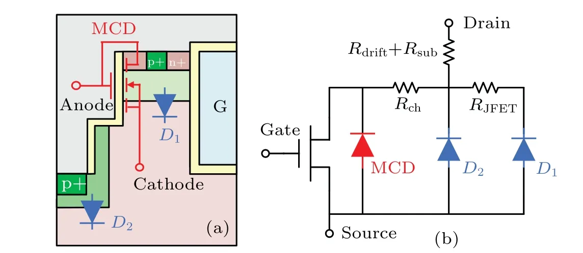
Fig.2.(a) Schematic view of the MOS-channel diode and two body diodes.(b)Equivalent circuit for the proposed MT MOS.
3.Results and discussion
Figure 3(a)shows the reverse current characteristics in the third quadrant for the three devices.Figure 3(b)illustrates the hole density contours and current flowlines.For the MT MOS in the initial stage,MCD turns on firstly as|Vds|increases and the hole current is zero.It verifies that the MT MOS operates in unipolar conduction mode since the current flows along the inversion layer of MCD as shown in Fig.3(b).The parasitic body diode turns on at|Vds|≈3.2 V and the MT MOS transfers to bipolar conduction mode with a sudden increase in the hole/total current.Therefore,the turn-on of the parasitic body diode is suppressed in the red shaded region.For the ST MOS,its integrated SBD also turns on prior to the body diode to conduct in unipolar mode.For the DT MOS,it conducts in bipolar conduction mode and the current flows through the parasitic body diode (shown in Figs.3(a) and 3(b)).As illustrated in Fig.3(b), the hole densities in the drift region for MT MOS(e.g.,110 cm-3)and ST MOS(e.g.,370 cm-3)are much lower than that of DT MOS(e.g.,3.1×1013cm-3),which confirms the unipolar mode instead of bipolar mode like that of the DT MOS.Obviously,theVF@Ids=-100 A/cm2of the MT MOS and ST MOS reduces to 1.70 V from 2.75 V of the DT MOS.The voltage transferring to the bipolar mode for MT MOS is larger than that for DT MOS,because the MCD suppresses the bipolar conductance modulation effect.
Figures 4(a) and 4(b) compare the forward conduction and blocking characteristics of the three devices.TheRON,spvalues for the MT MOS and DT MOS are 1.525 mΩ·cm2and 1.536 mΩ·cm2, respectively.The breakdown voltages (BVs)for the MT MOS and DT MOS are 1487 V and 1493 V,respectively.Both devices exhibit almost the same figure-of-merit(FOM=BV2/RON,sp)value about 1.45 GW/cm2.Therefore,the MT MOS almost does not degrade theRON,spor BV compared with the DT MOS.By the way, the slightly weakened output current capability of the MT MOS is due to stronger JFET effect caused by shallow source trench.It is favorable for improving the short-circuit ruggedness of the device.[15]For the ST MOS, theRON,spis 1.865 mΩ·cm2and its BV is just about 1210 V,because its electric field(E-field)modulation effect is weakened without the double trench.To further investigate the breakdown characteristic, theE-field distributions in the blocking state withVds=1200 V are shown in Fig.4(b).Related parameters have been optimized to keep theE-field peak in gate oxide (Eox-m) lower than 4 MV/cm for the MT and DT MOSFETs.[16,17]It shows that the source trench and P-region prevent the gate oxide bottom from premature breakdown, and the stepped-trench source further improves the electric field distribution in the MT MOS.However,theEox-min the ST MOS is larger than 4 MV/cm, owing to lack of source trench to modulate theE-field distribution.

Fig.3.(a)Reverse conduction I-V characteristics at Vgs =-5 V.(b)Hole density and total current flowlines distribution for three devices at Ids=-100 A/cm2.

Fig.4.(a) The I-V characteristics in forward conduction and blocking states.(b) Electric field contours at Vgs =0 V and Vds =1200 V in half-cell for the three devices.

Fig.5.(a)and(b)Forward blocking characteristics and(c)current flowlines distributions for the MT MOS and ST MOS with different NPB.
Figures 5(a) and 5(b) compare the forward blockingIVcharacteristics for the MT MOS and ST MOS with different P-body doping concentrations (NPB).Figure 5(c) illustrates the leakage current flowlines distributions extracted from theA,B,CandDpoints labeled in Figs.5(a) and 5(b).For MT MOS, the leakage current keeps a low value(about 10-17A) whenNPB≥1×1016cm-3, while significantly increases(about 5×10-12A)atNPB=1×1015cm-3.For the ST MOS,the blocking voltage significantly decreases whenNPB=4×1016cm-3.For both the devices, high leakage current and BV degeneration are caused by the punchthrough of the P-body in NPN(N+/P-body/N-drift),as shown in Fig.5(c).Therefore, both the MT MOS and DT MOS in this work adoptNPB=1×1016cm-3to ensure lowVFand high BV,and the ST MOS adoptsNPB=2×1017cm-3.
The reverse recovery characteristics are investigated by simulations with the inductive clamping double pulses test circuit shown in Fig.6(a).The purple or pink dashed arrows denote current paths when the upper arm MOSFET (device under test, DUT) is working in freewheeling or shutdown mode.The blue arrow denotes the reverse recovery current of DUT.Figure 6(b)illustrates that the reverse recovery waveforms of the MT MOS and DT MOS are almost the same atIload=100 A/cm2.However,at a highIload(e.g.,Iload=400,700 A/cm2),the reverse recovery current peak and reverse recovery time of the MT MOS are far less than those of the DT MOS.To investigate the mechanism,Fig.6(c)shows the hole concentration alongAA'cut line(in Fig.3(b))in reverse freewheeling mode.AtIload=100 A/cm2, the hole concentration of the DT MOS is much lower than the N-drift region doping (Ndrift), and thus its reverse recovery characteristic is the same as that of MT MOS.However,atIload=400 A/cm2and 700 A/cm2, the injected hole concentrations in DT MOS are higher than theNdrift,while the hole concentrations in MT MOS are still much lower than theNdrift.This is because the body diode in DT MOS is completely turned on at the largeIload(e.g.,Iload≥400 A/cm2),and then a large number of holes are injected into the drift region to realize the conductance modulation effect.However, the MT MOS relies on MCD to achieve reverse conduction,which could suppress the conductance modulation effect induced by the body diode.Thus,only a few holes are injected into the drift region and then the MTMOS shows much lower hole density even at the largeIload.Therefore, the MT MOS shows a much better reverse recovery characteristic than the DT MOS at a high current density,owing to much fewer excess carriers needed to be extracted.The reverse recovery characteristics of ST MOS are similar to those of the MT MOS, because both devices are in unipolar mode.Compared with the DT MOS, the decreased ratio of reverse recovery charge(Qrr)for the MT MOS increases from 2.55% atIload=100 A/cm2to 58.7% atIload=700 A/cm2as shown in Fig.6(d).It indicates that the MT MOS exhibits obvious advantages over the DT MOS at highIload.
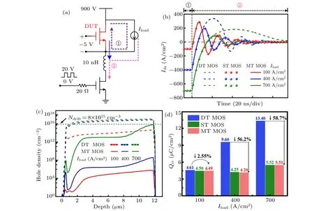
Fig.6.(a) Inductive clamping double pulse test circuit for the reverse recovery characteristics.(b) Reverse recovery waveforms.(c) Hole concentration in reverse freewheeling mode.(d)Reverse recovery charge(Qrr)under different Iload.
Figure 7(a)depicts the impacts ofNPBandtoxsonVFfor the MT MOS.Obviously,theVFdecreases with the decreasingtoxsorNPB.That is because the electronic barrier heights are lower for smallertoxsorNPBvalues, as the conduction band distribution along the MCD sidewall is shown in Fig.7(b).Then, it is easier to form the inversion layer to conduct the reverse current and realize a lowerVF.The area below the red dashed line in Fig.7(a) represents the optimal region, in whichVFvalue is lower thanVF=2.75 V of DT MOS.For a too highNPB,it is difficult to form the inversion layer and thus the PN body diode turns on to determine theVF, wherein theVFis above 2.75 V and is almost independent oftoxs.However,if theNPBis too low, the leakage current of the MT MOS in blocking mode will be too large,which is discussed in Fig.4.

Fig.7.(a) Influences of toxs and NPB on VF for MT MOS at Ids =-100 A/cm2.(b) Conduction band distributions along MCD sidewall with different NPB and toxs at Vds=0.
Figure 8(a) shows the impacts of theDSandLoffonVF.TheVFof the MT MOS decreases with the increasingDSowing to the lengthened electron accumulation layer path along the MCD sidewall.Also,the optimal value(>0.15μm)ofLoffcan reduce the spreading resistance and then a smallVFcan be obtained.It is noticeable that whenDSis larger than 0.9μm,theVFchanges just slightly with the varyingLoff,as the shaded region shown in Fig.8(a).The influences of the work function (Wm) of source metal onVFand reverse conductionI-Vcharacteristic are depicted in Fig.8(b).As the work function increases,theVFincreases while the|Vds|required to transfer to the bipolar conduction mode decreases,because the mutual depletion effect induced by the source metal is enhanced.Considering the influences of these parameters,an optimizedVFof 1.70 V atNPB=1×1016cm-3,toxs=10 nm,DS=1μm andLoff=0.2 μm is achieved.In this work, the work function value of the source contact metal is set to 4.25 eV,[8]and the mentioned work function values and their source metal can refer to Refs.[8,18-22].
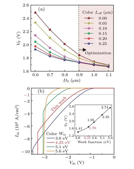
Fig.8.Influences of the(a)DS and Loff,and(b)work function(Wm)of source metal on VF for the MT MOS at Ids=-100 A/cm2.

Fig.9.Short-circuit characteristics for the MT MOS and DT MOS.
Figure 9 shows the short-circuit waveforms.The failures of the MT MOS and DT MOS are detected when the gate turns off andIdssharply rises,which is caused by the high heat generated in the short circuit process and unable to give away in time.Owing to its lower saturation current, the short-circuit time of the MT MOS extends to 7 μs from 5 μs of the DT MOS.As shown in Table 2,the MT MOS achieves better comprehensive performances than other two devices.
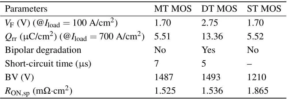
Table 2.Performance comparison of the three devices.
4.Conclusion
A novel SiC MOS with an integrated MOS-channel diode is proposed and studied by TCAD simulations.The MCD can realize a lowVFin unipolar reverse conduction mode and then suppress the bipolar degradation.The simulation results show that the MT MOS exhibits a significant improvement in both the forward and reverse characteristics.TheVFof MT MOS is 38.2% lower than that of DT MOS.The reverse recovery chargeQrrof MT MOS is 58.7% lower than that of the DT MOS atIload=700 A/cm2.Therefore,the reduced reverse recovery loss is obtained for MT MOS,especially in the case of large load currents.Meanwhile, the MT MOS preserves the same advantages as those of DT MOS in forward conduction and blocking characteristics, and increases the BV by 277 V compared with the ST MOS.
Acknowledgements
The authors appreciate the support by the Science &Technology Program(High voltage and high power SiC material,devices and the application demonstration in power electronic transformers) of the State Grid Corporation of China Co.Ltd.
Project supported by the National Key Research and Development Program of China(Grant No.2016YFB0400502).

- Chinese Physics B的其它文章
- Analysis of cut vertex in the control of complex networks
- Atlas of dynamic spectra of fast radio burst FRB 20201124A
- Investigating the characteristic delay time in the leader-follower behavior in children single-file movement
- Micro-mechanism study of the effect of Cd-free buffer layers ZnXO(X =Mg/Sn)on the performance of flexible Cu2ZnSn(S,Se)4 solar cell
- Thermally enhanced photoluminescence and temperature sensing properties of Sc2W3O12:Eu3+phosphors
- Heterogeneous hydration patterns of G-quadruplex DNA