Transition-edge sensors using Mo/Au/Au tri-layer films
2023-03-13 09:20:16HubingWang王滬兵YueLv呂越DongxueLi李冬雪YueZhao趙越BoGao高波andZhenWang王鎮
Chinese Physics B 2023年2期
Hubing Wang(王滬兵) Yue Lv(呂越) Dongxue Li(李冬雪)Yue Zhao(趙越) Bo Gao(高波) and Zhen Wang(王鎮)
1State Key Laboratory of Functional Materials for Informatics,Shanghai Institute of Microsystem and Information Technology,Chinese Academy of Sciences,Shanghai 200050,China
2CAS Center for Excellence in Superconducting Electronics(CENSE),Shanghai 200050,China
3University of Chinese Academy of Sciences,Beijing 100049,China
Keywords: transition-edge sensors,proximity effect,electroplating
1.Introduction
Transition edge sensors(TESs)are highly sensitive photon detectors that rely on the sharp resistance variation at the superconducting-transition edge to detect incident photons.[1]TES x-ray microcalorimeters with high energy resolving power have been implemented widely in x-ray astronomy and synchrotron radiation light sources.[2-5]The energy resolution of a TES depends strongly on the transition temperature (Tc)of the superconducting film.A TES-based microcalorimeter is usually made from a superconducting film withTc<100 mK.The proximity effect between a superconducting and a normal metal film is an effective method to grow a low-Tcsuperconducting film.[6]Mo/Au and Mo/Cu are typical material combinations for TESs because both bilayer systems are robust with regard to diffusion and the formation of an intermetallic phase.[7-9]A TES microcalorimeter usually requires a low normal-state resistance to reduce internal thermal fluctuation noise.It is straightforward to grow a Cu film with low resistivity via sputtering.However,to reduce its resistivity,an Au film must be prepared using evaporation methods instead of sputtering, which usually requires a separate deposition system and increases costs.Cu films suffer from oxidation,while Au films do not,which ensures a long-time stability of an Mo/Au TES.[10]To prepare Mo/Au bilayer films,one can deposit the Mo film first using evaporation or sputtering, and then transfer the sample to another chamber to evaporate gold without breaking vacuum.The interface between the Mo and the Au layer can therefore be kept clean.[11]An alternative way is to deposit the Au layer in a separate evaporator, which requires careful ion cleaning before the deposition to obtain a transparent and uniform Mo-Au interface.[12]A third method involves using Mo/Au/Au tri-layer films,in which a thin protective Au layer is sputtered on top of the Mo film before breaking vacuum, and the second Au layer is then deposited via evaporation.The protective Au layer improves the transparency of the Mo-Au interface,makes the ion-cleaning process less critical,and increases the uniformity of the tri-layer.[13]In this work,we use Mo/Au/Au tri-layer films and improve the fabrication process by integrating the patterning of the TES sensors while forming the tri-layer films.This reduces the complexity of detector fabrication.We report the electrical characterization of the detectors and demonstrate their energy-resolving capability using a55Fe radioactive x-ray light source.
2.Device fabrication
2.1.Mo film preparation and the first layer of gold
In experiment,the Mo film and the first layer of Au were deposited successively via direct-current magnetron sputtering(CMS 18, Kurt J.Lesker, US)on a four-inch Si wafer with a 300-nm-thick SiO2layer and a 500-nm-thick SiNxlayer.The Si substrate was cleaned with Ar+ion bombardment before the deposition to improve film adherence.Because the thickness of the Mo was comparable to the electron mean free path,the resistivity andTcwould be affected by a reduced thickness.Hence,the Mo film thickness was approximately 45 nm to ensure stability.[14]After the Mo deposition, the 30-nm protective Au layer was immediately sputter-deposited in the same chamber.The Mo and Au deposition parameters are listed in Table 1.
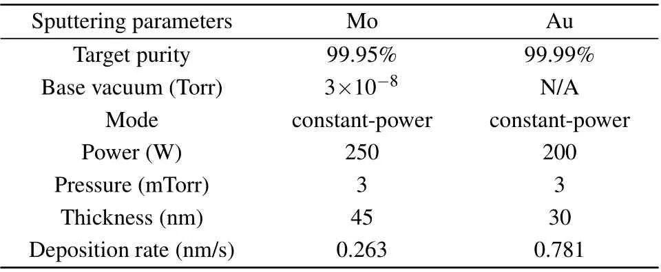
Table 1.Deposition parameters for Mo and Au layers.
2.2.Patterning the Mo/Au layer and depositing the second Au layer
The Mo/Au bilayer was patterned into a square form with connecting leads using photoresist (LC100A) as an etching mask.The thickness of the photoresist was 1.8μm,and the bilayer was chemically wet-etched using gold etchant GE-8148 at 20°C and etching rates of 5 nm/s for Au and 10 nm/s for Mo.The wafer was then rinsed with deionized water and dried under N2.
The second Au layer was thermally evaporated at 1.5 °A/s(PVD75,Kurt J.Lesker)at a base pressure of 1.5×10⁻⁷Torr.The wafer was cooled during evaporation and the Au film was deposited after Ar+ion cleaning.The process flow chart is shown in Fig.1.To prevent the formation of a superconducting short cut at the edge of the Mo-Au film,the top gold layer is slightly wider than the bottom Mo-Au layer.
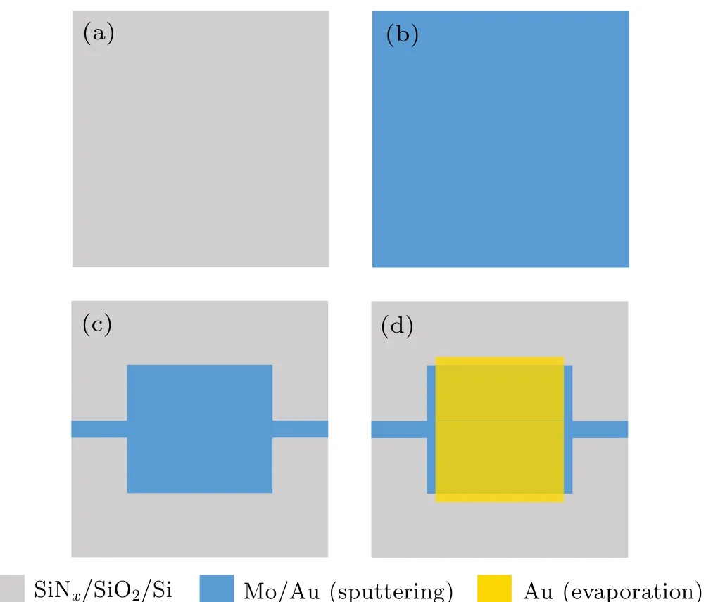
Fig.1.Schematic of Mo/Au/Au tri-layer fabrication: (a) ion-cleaning SiNx/SiO2/Si substrate,(b)sputtering Mo/Au(protective)film,(c)wetetching Mo/Au film,(d)depositing the second Au layer.
2.3.Fabrication of overhanging photon absorber and SiNx window
For a TES designed to detect soft x-rays with an efficiency being not less than 70%at 5.9 keV,we used pure gold as the absorber material,several-micrometers-thick gold was needed to have sufficient stopping power.Theoretical calculations shown in Fig.2 indicate that a 2.5-μm-thick Au film had a more than 89%quantum efficiency for 5.9-keV photons.[15]To make such thick gold films,we used an electro-plating system(JDY-3,CETC)that accommodated a four-inch wafer.To accelerate the thermalization of the absorber,it was necessary to increase the thermal conductivity, which increased with electrical conductivity.A 346 nm/min deposition rate helped to reduce the resistivity of the gold film to 1.3×10⁻⁹Ω·m, and the residual resistance ratio was 13.4.
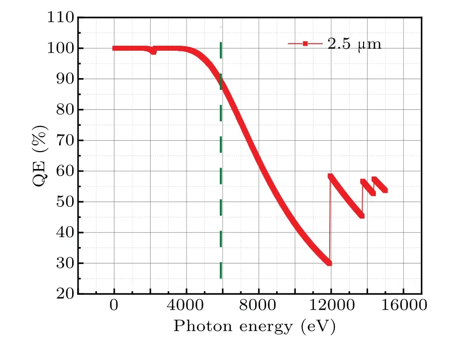
Fig.2.Quantum efficiency of 2.5-μm Au absorber.The green dashed line is the 5.9-keV line of Mn Kα.
To increase the photon-sensitive area of the detector and to reduce the electrical coupling between the absorber and the Mo-Au-Au film,we fabricated an overhanging gold absorber supported by Au stems contacting the superconducting film and the SiNxmembrane.The overhanging structure was fabricated using a two-layer photoresist lift-off and electro-plating process.[16]In the first step, a photoresist evaporation mask was patterned to define the 2-μm-high supporting stems and to form the electroplating seed layer,as shown in Fig.3(a).After the metallization,the second photoresist layer was spin-coated and patterned without removing the first resist layer.The main body of the absorber and the supporting stems were electroplated to a thickness of approximately 2.5 μm.Both resist layers were then removed with acetone and a plasma process.A mushroom-like overhanging absorber was thus formed.Figure 3(b) shows a close-packed overhanging absorber array,
where the inset shows a magnified scanning electron microscope image of the edge of the absorbers.
The final step of the detector fabrication was to define the SiNxmembrane substrate to reduce the thermal conductance between the detector and the thermal bath.A deep siliconetching process (DSiE) was used (Estrelas 100, Oxford instruments, GB).[17]Before the process, the entire front side of the wafer was protected with 6 μm-thick photoresist.The DSiE process uses 8μm-thick photoresist as the etching mask.The exposed Si was etched with an SF6plasma and passivated with a C4F8plasma in sequence.The etching depth and sidewall steepness were controlled by fine-tuning the durations of the etching and passivation.Three hundreds of etchingpassivation cycles were used to obtain a 400 μm depth over 30 min.After the DSiE process,the photoresist was removed with acetone.
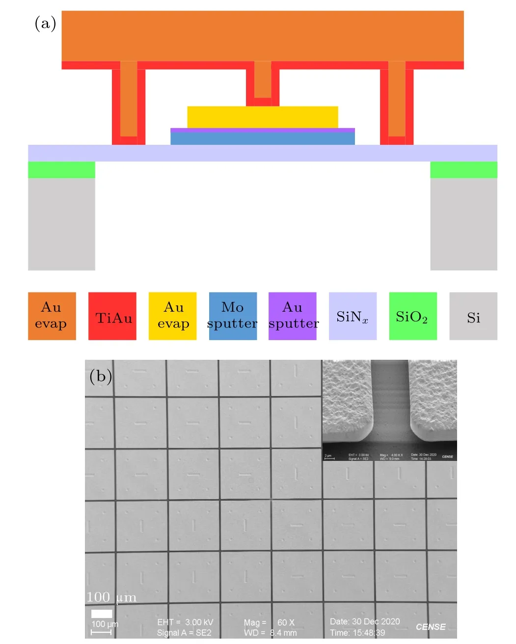
Fig.3.(a) Schematic depiction of a transition-edge sensor with absorber,the corresponding material is listed below.(b)Scanning electron microscope image of electro-plating mushroom Au absorber array.The inset shows the magnified view of the gap between two absorbers.
3.Characterizations of the sensors
The fabricated sensor arrays contained 4×4 Mo/Au TES pixels with the integrated Au absorber.Detailed geometric parameters are listed in Table 2.We characterized these devices by acquiring small-current resistance-temperature (RT) curves and current-voltage (I-V) curves in an adiabatic demagnetization refrigerator.The latter were acquired with a two-stage SQUID readout system from STAR cryo-electronics LLC.Figure 4(a)shows theR-Tcurve obtained by measuring the resistance using a small excitation current while sweeping the bath temperature in 1-mK steps.The normal-state resistance and the superconducting transition temperature were approximately 16 mΩ and 90 mK, respectively.Figure 4(b)shows a variety ofI-Vcurves measured at various bath temperatures.For clarity,onlyI-Vcurves from a single pixel are shown.By calculating the Joule heating power at 80%Rn,
where the current dependence of the detector resistance was negligible, and the resistance was assumed to be only dependent on the temperature,[18]we plotted the power vs.bath temperature curves (P-Tbath) shown in Fig.4(c), and determined the thermal conductanceGto the heat bath using the following first equation.[19]T0is the detector temperature at the working point(80%Rn),G(T0)is the thermal conductance at that temperature, andnis the exponent of the power flow to the heat bath.The three parameters can be fitted from the curves plotted in Fig.4(c).We have
Using the thermal conductance, we calculated the nonequilibriumR-Tcurves by translating the Joule-heating power into the temperature variation.Figure 4(d) plots theR-Tcurves deduced from theI-Vcurves measured at the 65-mK bath temperature.TheseR-Tcurves indicated how the detector resistance evolved with current heating.The inset of Fig.4(d)shows a 4×4-pixels Mo/Au/Au TES array.

Table 2.TES electro-thermal parameters.
We summarized the geometric and electro-thermal detector parameters in Table 2.The heat capacityCwas roughly estimated from the absorber size and the bulk value of the materials
whereρ/Ais the ratio of density to atomic weight,γis molar specific heat,Vis the volume of Au absorber,andTis the temperature at the working point.
The natural time constant could be calculated from the heat capacityCand the thermal conductanceG,τ=C/G.The theoretical energy resolution in the small-signal limit and effective time constant is given by
where the loop gainLI=PJ0α/GT0, andPJ0is the power of working point.

Fig.4.(a) The R-T curves with small excitation current of an Mo/Au/Au transition-edge sensor (TES).(b) Typical I-V curves of a TES pixel 3.The red dashed line is 80% Rn.(c) The measured and fitted P-Tbath curves of three sensors on the same chip with identical design.(d)Non-equilibrium R-T curves of three Mo/Au/Au TESs on the same chip.
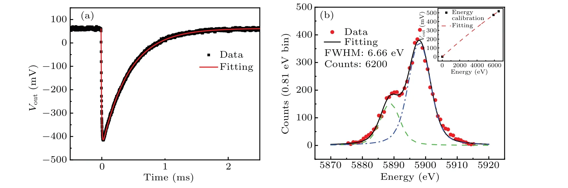
Fig.5.(a)Typical pulse of an Mo/Au/Au transition-edge sensor(TES).The black line was the measured pulse,the red line was the double-exponent fit to V =A(e-(t-t0)/τel-e-(t-t0)/τeff)+Voffset.(b)Energy spectrum of 5.9-keV Mn Kα x-ray.The red dots are the original spectrum.The black line is the fitting curve using the convolution of the detector Gaussian response function with the natural line profile of the incident x-ray photons.The blue dash-dotted line and the green dashed line are the convolution of the fitted Gaussian detector response function with the natural line profile of the Mn Kα1 and Kα2 emission lines,respectively.The inset shows the pulse amplitude-photon energy calibration curve.
The detector performance was characterized by using a55Fe radioactive source.The activity of the source is approximately 27μCi.The source was placed inside the cryostat,and the average measured count rate for a single TES pixel was approximately 1 count/s which is limited by the x-ray source.The detector bias current was supplied by a signal generator in series with a 1-kΩ resistor.
The bath temperature was set to 50 mK and the TES was biased at 15%Rn.A typical signal pulse is shown in Fig.5(a).The whole pulse duration time is approximately 2 ms and the effective decay timeτeffwas only 268 μs because of strong electro-thermal feedback, from which we could deduceα.From the pulse duration,we estimate that the maximum count rate of a single-pixel detector can reach up to 500 Hz assuming no pulse pile-up.The pipeline to deduce the energy resolution of the TES, named as the instrumental energy resolution, involves three steps.First, an optimal filter is built to digitally filter the raw signal pulses and extract the pulse height of each individual pulse.[20]Then the pulse height data(in units of V)is translated into the photon energy using the calibration curve shown in the inset of Fig.5(b).The voltage-photon energy calibration curve is built using the characteristic emission lines(KαandKβ)of Mn.The energy spectrum histogram is plotted as red dots in Fig.5(b).To deduce the instrumental energy resolution,we need to exclude the contribution of the natural line profile of the incident x-ray photons.[21]The black solid line in Fig.5(b)is the fitting curve by convolving the detector response function(assumed to be a Gaussian function)with the natural line profiles.The deduced instrumental energy resolution is 6.66 eV.The blue dotted and the green dashed lines in Fig.5(b)show the convolution of the fitted Gaussian detector response function with the natural line profile of theKα1andKα2emission lines.
4.Discussion
The instrumental energy resolution calculated above is 6.66 eV,which was worse than the theoretical value of 1.6 eV shown in Table 2 calculated from the electro-thermal parameters of the sensor.The discrepancy between the measured and calculated energy resolutions could be attributed to several factors.First,the deduction of the electro-thermal parameters was not very accurate,especially for the calculated heat capacity.Complex impedance measurements could better characterize the electro-thermal parameters of the sensors.[22]Secondly,we did not include the contribution of excess noise in the theoretical calculation of the energy resolution.Characterization of the excess sensor noise will be reported elsewhere.By adjusting the sensor size and adding certain metal structures we could reduce degradation of the energy resolution caused by the excess noise.[23]Lastly, the instrumental energy resolution discussed above still contains the noise contribution of the SQUID amplifier and its readout electronics.For the moment the SQUID noise is not negligible compared to the TES detector noise.A SQUID readout system with lower current noise would also help to improve the measured energy resolution.These studies are still on-going.
Acknowledgements
Project was supported by the National Key Research and Development Program of China (Grant No.2017YFA0304000), the Shanghai Municipal Science and Technology Major Project(Grant No.2017SHZDZX02),China National Space Administration (CNSA) (Grant No.D050104), and the grant for low energy gamma-ray detection research based on SQUID technique.The nanofabrication work was supported by the Superconducting Electronics Facility(SELF)of Shanghai Institute of Microsystem and Information Technology, Chinese Academy of Sciences.We thank Liwen Bianji(Edanz)(www.liwenbianji.cn)for editing the language of a draft of this manuscript.

- Chinese Physics B的其它文章
- Analysis of cut vertex in the control of complex networks
- Atlas of dynamic spectra of fast radio burst FRB 20201124A
- Investigating the characteristic delay time in the leader-follower behavior in children single-file movement
- Micro-mechanism study of the effect of Cd-free buffer layers ZnXO(X =Mg/Sn)on the performance of flexible Cu2ZnSn(S,Se)4 solar cell
- Thermally enhanced photoluminescence and temperature sensing properties of Sc2W3O12:Eu3+phosphors
- Heterogeneous hydration patterns of G-quadruplex DNA