石墨烯等離激元時間晶體中的慢光
2022-09-07 06:55:08卓立強莊鳳江蘇少堅林志立邱偉彬
中國光學 2022年4期
何 真,卓立強,李 志,莊鳳江,蘇少堅,林志立,邱偉彬
(華僑大學 信息科學與工程學院, 福建 廈門 361021)
1 Introduction
The slow light technology has attracted more and more attention due to its quite broad potential application prospect in optical field regulation and optical storage devices[1-3]. Controlling the structure dispersion to realize slow light is one of the commonly used technologies at present. The main method of this technology is to control the light group velocity by designing a slow optical waveguide with a specific structure. Slow light generated in such photonic crystal waveguides has been observed in several studies[4-5]. However, in the previous slow optical waveguide structure, when the group velocity becomes slow, its supported bandwidth is very narrow, and it is also accompanied by a huge group velocity dispersion effect. Scheuer J.et al. used a complex coupled resonant optical waveguide to achieve internal dispersion compensation and solved the problem of distortion[6]. In recent years, Surface Plasmon Polaritons (SPPs) waveguides have been used to realize slow light, which can achieve higher slow light capacity with a fixed structure, but the adjustment of slow light performance is limited[7]. In addition, the large group velocity dispersion effect of the chirped structure can cause seriously distortion of the optical signal, and the device has a limited operating frequency range[8]. Furthermore, the structural design of traditional slow-light devices is complicated and their tunability is poor once the structure is fixed, which limits their practical applications.
Photonic crystals have good topological band effects, and their topological concepts have great potential in the application of photonics, which has attracted extensive attention. Topological photonic structures have subverted some conventional views on wave propagation and manipulation. Applying topological photonic crystals to wave propagation makes it possible to realize new photonic devices with specific funtions, such as sharp bending waves without reflection, robust delay lines, spin polarization switches and non-reciprocal devices[9]. Recently, Chen Xiaodonget al. proposed and proved that the valley states in topological photonic crystals can be used as topological protection to realize light transmission. The design is to place two topological photonic crystals with different topological structures in mirror images to form an interface that can achieve topological protection[10]. Later, Yoshimiet al. proposed a method to realize topological slow optical waveguides in valley photonic crystals[11].The waveguide structure is based on a semiconductor substrate to realize slow light transmission with a group index greater than 100 in the topological band gap range, but the manufacturing process is complex, and the structure has no tunability and does not involve the change of field strength caused by slow light. With the deepening of research, it is found that the topological band gap structure of valley state can be realized in photonic time crystal materials whose refractive index changes periodically with time[12]. The method is that by breaking the crystal time translation symmetry, photonic time crystals can achieve topologically non-trivial phases[13-15],thereby affecting the propagation of light in the crystal.
It is well known that graphene has unique electrical and optical properties, especially it supports surface plasmonic excitation waves, and has relatively low ohmic loss and high tunability[16]. Jinet al.designed monolayer graphene with periodic patterns to achieve topological unidirectional boundary transport by introducing a static magnetic field[17].Later, Wang Yanget al. realized topological valley plasmonic transport in bilayer graphene metasurfaces for sensing applications[18]. Recently, Guo Xianget al. designed a graphene SPP equivalent twodimensional photonic crystal slow light waveguide through photonic crystal line defects, and achieved slow light modulation through the gradual change of chemical potential of graphene in space[19]. Likewise, it is very important to realize the modulation of the slow light transport in the valley state topology of graphene plasmonic crystals in time. In this paper, we propose a novel approach to achieve topological slow light transport in waveguides constructed from graphene plasmonic time crystals. Two-dimensional graphene plasmonic time crystals consist of a set of graphene nanodisks periodically arranged in a honeycomb pattern. By controlling the periodic change of the chemical potential of graphene with time, the time-translational symmetry of graphene plasmonic time crystals is broken. Numerical simulations show that the plasmonic time crystal band gap can open and close periodically with time. Further, we find that the Zigzag edges can support near-zero electromagnetic transport group velocities within the topological bandgap. Numerical simulation results of electromagnetic transmission in slow light waveguide show that the topological waveguide can generate slow light. The advantages of this method are simple structure, good field enhancement effect and dynamic tuning ability, which provides a new way for dynamically realizing optical field regulation.
2 Numerical simulation methods and models
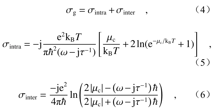
In this paper, a valley state topological slow optical transmission waveguide is implemented based on graphene plasmonic time crystals. As shown in Fig. 1(a) (Color online), the waveguide adopts the Zigzag structure topological interface as the transmission channel, and the top is composed of graphene nanodisks. Graphene is in contact with air,SiO2is selected as the background material, and Si as the substrate material. It can be seen from the cross-sectional view of the waveguide in the figure that the bias voltage is applied to the graphene nanodisk and the silicon substrate. The silicon pillars are arranged in a triangular lattice, andV1(t),V2(t)andV3(t) are the bias voltages applied to the graphene nanodisks, respectively. This method is based on the photonic crystal realization mechanism of the graphene plasmonic exciton[20]. When the distance between graphene and the substrate is constant, the chemical potential of graphene can be changed by changing the applied voltage.
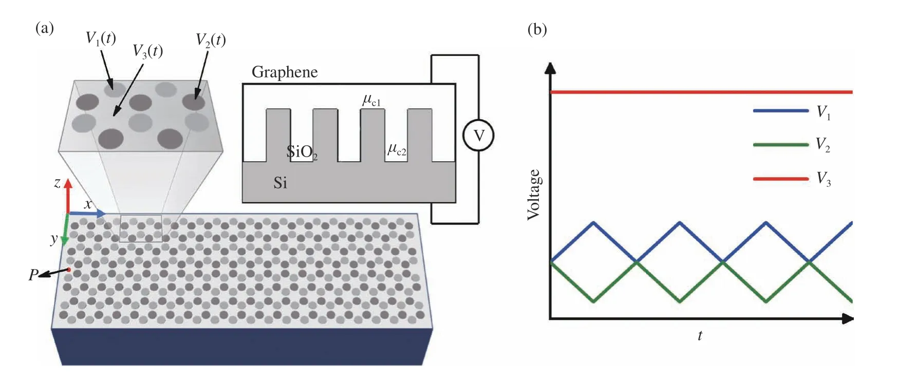
Fig. 1 (a) The three-dimensional schematic of slow light waveguide, with a single layer of graphene nanodisks at the top. The graphene is exposed to air on the top, the background material is SiO2, and the substrate material is Si. Different graphene nanodisks are applied with different bias voltages: V1(t), V2(t) and V3(t). The diagram on the right shows how voltage is applied. (b) The graphene nanodisk’s external bias voltage changes periodically with time圖1 (a) 慢光波導的三維示意圖,頂部是單層石墨烯納米盤。石墨烯與空氣接觸,背景材料是 SiO2,襯底材料是Si。對不同的石墨烯納米圓盤分別加載不同的偏置電壓:V1(t),V2(t)和V3(t),右上圖為電壓的施加方式。(b) 石墨烯納米盤外加偏置電壓隨時間周期性變化的曲線
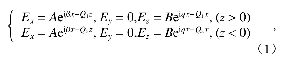
It is assumed that the relative permittivity of the surrounding environment of graphene is εr1and εr2, respectively. The relative permittivity of the substrate SiO2is εr1=3.9, and the relative permittivity of the air on the upper surface of the graphene is εr2=1. In our numerical simulation, the TM mode is considered and the electric field form of TM mode is assumed to be[21]:
where ε0is the vacuum permittivity in free space,ω is the angular frequency of the plasmon, andcis the propagation speed of light in vacuum. In the whole calculation process, we only consider the case of the propagation constant β?,so equation (2) can be simplified to the following form[23]:
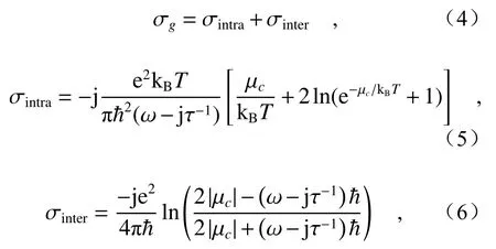
where β is the propagation constant based on graphene SPP, the surface conductivity of graphene σgcan be adjusted with temperatureT, chemical potential μc, scattering rate τ and angular frequency ω,which consists of two parts: intra-band electron scattering σintraand inter-band electron transition σinter, according to Kubo Formula[23]:
where kBis the Boltzmann constant, e is the charge of the electron, andhˉ is the reduced Planck constant.Specifically, the chemical potential of graphene μccan be effectively tuned by an externally applied voltage[20-21,24-25].
wherevFis the Fermi velocity,Coxis the gate capacitance[26], andVg(t) is the applied voltage that changes periodically with time. In this paper, the curve of the applied bias voltage of graphene nanodisk changing periodically with time is shown in Fig. 1(b) (Color online). By changing the bias voltagesV1(t),V2(t) andV3(t) applied to the graphene nanodisks, the graphene chemical potentials μc1(t), μc2(t) and μc3(t) are changed.
3 Numerical simulation results and discussion
3.1 Graphene plasmonic time crystal model and properties
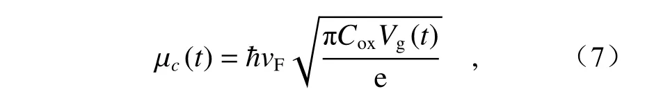
First, we explored the energy band topology of 2D graphene plasmonic crystals composed of graphene nanodisk arrays arranged in a triangular lattice. The time crystal structure of graphene plasmon is shown in Figure 2 (a). The dotted line area is the crystal cell, and the solid line part is the Brillouin region of the crystal, where Γ-M-K-Γ is the reduced wedge of Brillouin region,ais the crystal lattice constant,a=40 mm, and the radius of graphene nanodisk is expressed asrandr=0.21a.μc1, μc2and μc3are the chemical potentials of different graphene nanodiscs, respectively. From equation (7), it can be seen that the chemical potentials of these graphene nanodiscs can also change periodically with time, which can be written as μc1(t) ,μc2(t) and μc3(t)[27-29]. The chemical potential of graphene nanodisks can be flexibly controlled in time by applying periodic changed bias voltage ofV1(t),V2(t) andV3(t). Here, we calculate the energy bands of graphene plasmonic time crystals at several moments in one cycle, as shown in Fig. 2(b)(Color online), where the black line depicts that,whent=0 s (i.e. Δμc=μc1-μc2=0 eV), the chemical potentials of the graphene nanodisk are μc1= μc2=0.3 eV and μc3=0.6 eV, respectively, the two energy bands degenerate at theKpoint and intersect at the Dirac point, and there is obviously no band gap.During the periodic change of chemical potential with time, the time-translation symmetry of the graphene plasmonic time crystal is broken, the Dirac cone dispersion will be split, and the band gap will be opened[30]. The green, blue and red curves in Fig. 2(b) depict the band structures of the following three time nodes:t1=1 e-12s (i.e.Δμc= 0.1 eV),t2= 1.5 e-12s (i.e. Δμc= 0.12 eV) andt3=2 e-12s (i.e. Δμc=0.14 eV), respectively. It is clear that the crystal band gap undergoes a process from closing to opening over time. It is worth noting here that this graphene plasmonic time crystal energy band change over time can be performed without changing the geometry.
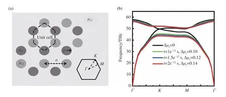
Fig. 2 (a) Schematic diagram of graphene plasmon time crystal structure. (b) Energy band diagrams of graphene plasmon time crystals at four different moments in a cycle of external bias voltage change圖2 (a) 石墨烯等離激元時間晶體結構示意圖。(b)在一個外加偏置電壓變化周期內(nèi),石墨烯等離激元時間晶體在4 個不同時刻的能帶圖
In order to verify the properties of graphene plasmonic time crystals, a numerical simulation study is designed in this work. As shown in Fig. 3(d), in a region composed of graphene plasmonic time crystals, an excitation source is placed at pointP, and the relationship between the chemical potentials of graphene nanodisks satisfies the variation law shown in Fig. 3 (a). Here, electromagnetic waves with a frequency of 46.50 THz are excited from the excitation source. We further explored the change trend of crystal energy band gap with the change of graphene chemical potential. By analyzing the opening and closing of the band gap, the propagation phenomenon occurs when the frequency of the excitation wave is in the conduction band; however, when the frequency is in the band gap, the wave will not propagate in this time interval[31-33]. The simulation results are shown in Figure 3(Color online), in which screenshots are taken of the electric fields at four time nodes during the transmission process. With the periodic change of Δμcin time, the transmission and inhibition alternate phenomenon occurs in the timing oftb=3.20 e-12s,tc= 4.16 e-12s,td= 5.82 e-12s andtf=8.24 e-12s, respectively. This result can well illustrate that the graphene plasmonic time crystal can realize the periodic opening and closing of the energy band gap with time by periodically adjusting the chemical potential.
Fig. 3 (a) When μc3=0.6 eV, the relationship between Δμc and t. (d) A region composed of 5×10 graphene plasmon time crystals. P is the position of the excitation source. (b), (c), (e) and (f) Screenshots of four moments in the propagation process at the time nodes of t b =3.20 e-12 s, t c= 4.16 e-12 s, t d =5.82 e-12 s and t f=8.24 e-12 s, respectively圖3 (a) 當 μc3= 0.6 eV 時, Δμc與t 的關系。(d) 5×10 石墨烯等離激元時間晶體組成的一個區(qū)域,P 是激發(fā)源的位置。(b),(c),(e)和(f)是傳播過程中4 個時刻的截圖,時間節(jié)點分別是 t b =3.20 e-12 s, t c= 4.16 e-12 s, t d =5.82 e-12 s 和t f=8.24 e-12 s
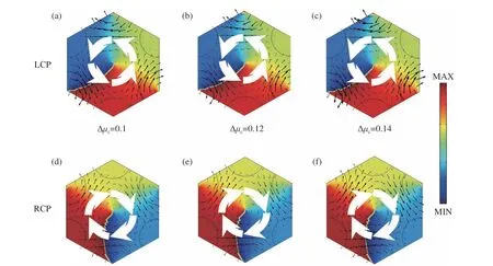
Fig. 4 The phase distributions of Left-handed Circularly Polarized (LCP) and Right-handed Circularly Polarized (RCP) of the time crystal appear at point K, which are expressed as the component of the electric field in the direction Z and the inplane Poynting vector (Px, Py). (a) and (d) the phase distribution diagram of point K at the time of Δμc=0.1 eV; (b) and(e) the phase distribution diagram of point K at the time of Δμc=0.12 eV; (c) and (f) the phase distribution diagram of point K at the time Δ μc=0.14 eV圖4 時間晶體在K 點分別出現(xiàn)了左旋圓極化(LCP)和右旋圓極化(RCP)的相位分布,表示為電場在Z 方向上的分量和面內(nèi)坡印亭矢量(Px, Py)。(a)和(d)是在 Δμc= 0.1 eV 時刻,K 點的相位分布圖;(b)和(e)是在 Δμc=0.12 eV 時刻,K 點的相位分布圖;(c)和(f)在 Δμc=0.14 eV 時刻,K 點的相位分布圖
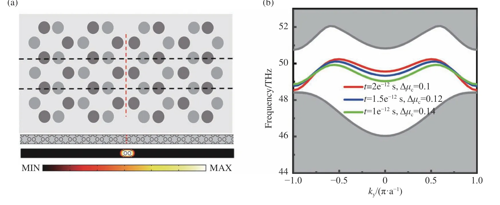
Fig. 5 (a) Schematic diagram of the Zigzag interface based on graphene plasmon time crystals, in which the bottom is the calculation model of the finite period super cell unit and the simulation electric field distribution results. (b) The dispersion curves of the Zigzag interface mode at different times圖5 (a) 基于石墨烯等離激元時間晶體構成的Zigzag 邊界示意圖。其中,底部分別是有限周期超胞單元的計算模型和仿真電場分布結果。(b)不同時刻下Zigzag 邊界模的色散曲線
3.2 Zigzag topological boundary structure theory and model
When the time-translational symmetry of the graphene plasmonic time crystal is broken, the Dirac cone dispersion is not preserved. From the point of view of group theory, when the inversion symmetry is broken, the group symmetry of the point (KorK′) will be reduced fromC3vtoC3. In the energy band, the Dirac cone is destroyed, and the two energy bands originally degenerated to the pointKwill be opened[34-35]. By analyzing the change of the orbital angular momentum at the valley of the energy band after the energy band is opened, we obtain the phase distribution at pointKat time oft1=1 e-12s (i.e.Δμc= 0.1 eV),t2= 1.5 e-12s (i.e. Δμc= 0.12 eV) andt3=2 e-12s (i.e. Δμc=0.14 eV). As shown in Figure 4(Color online), it can be seen that, at different times,the two energy bands appear the phase distribution of Left-handed Circular Polarization (LCP) and Right-handed Circular Polarization (RCP) at the degenerate pointK, respectively, that is, in the process of Δ μcchanging with time, the energy valley at any moment has the circularly polarized orbital angular momentum in the opposite direction after the time crystal energy band is opened. Therefore, we construct electromagnetic transport at the topological edge through electromagnetic modes that can be loaded with different orbital angular momentums,which provides a theoretical basis for the use of topological boundary to construct slow light waveguides.
In this study, Zigzag topological boundaries are used to construct slow light waveguides. This topology is constructed from graphene plasmonic time crystals, which generate “ temporal topological boundary states”, they are temporal analogs of topological edge states[13]. Breaking the time-translational symmetry of graphene plasmonic time crystals will lead to the opening of Dirac points at band degeneracy, thus forming a full band gap in which topologically protected boundary modes exist. The red dotted line in Figure 5(a) (Color online) is the Zigzag topology interface. By sampling the area within the black dotted line, a finite period (N=19) supercell model is established in the commercial simulation software COMSOL Multiphysics. Part of the simulation results are shown at the bottom of Fig. 5(a) (Color online), and it can be seen that the electric field distribution is concentrated at the boundary. We also calculated the dispersion relation of this boundary mode at different times(Fig. 5(b)), and the gray area represents the projected body energy band diagram. Fig. 5(b) also depicts the projected energy bands of three boundary states at the timet1= 1 e-12s,t2=1.5 e-12s andt3= 2 e-12s[36]. Obviously, when Δμcchanges with time, there is always a corresponding boundary state at each moment, which means that the time simulation based on the Zigzag topology boundary state of the graphene plasmon time crystal is realized.
3.3 Slow light phenomenon and field enhancement effects
By further analyzing the dispersion relation of the above boundary modes, we can deduce a phenomenon that the group velocity is zero (slow light)at the extreme point of the dispersion curve. In order to better study the group velocity of guided modes existing in this boundary state, the partial dispersion curves at three different times are plotted in Fig. 6(a) (Color online). It is obvious that the dispersion is accompanied by severe bending, which leads to the existence of slow light mode in the gap.Based on the dispersion curves of these boundary modes, the change curve of the group velocity with angular frequencywcan be calculated with the relationshipvg=dω/dk[37-38]. As shown in Figure 6(b)(Color online), the red curve is the group velocity att1= 1 e-12s and Δμc=0.1 eV, the group velocity tends to zero, and the frequency to 50.237 0 THz. Att2= 1.5 e-12s and Δμc=0.12 eV, the electromagnetic wave group velocity is close to zero at the frequency of 50.114 9 THz, which is depicted in Fig. 6(b) by the blue curve. Att3=2 e-12s and Δμc=0.14 eV, the group velocity is close to zero at a frequency of 49.929 2 THz, which is marked by the green curve. Numerical calculation results show that the group velocity of electromagnetic waves with different frequencies reach zero at different moments, that is, the topological boundary can realize slow light that its certain frequency electromagnetic wave group velocity near zero at different moments.
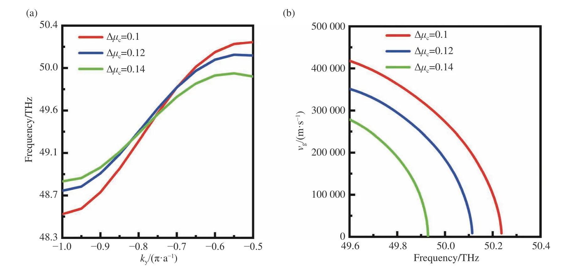
Fig. 6 (a) The boundary mode dispersion curve supported by the topological boundary under different Δμc. (b) The relationship between group velocity and frequency under different Δμc圖6 (a) 不同 Δμc下 拓撲邊界所支持的邊界模色散曲線。(b)不同 Δμc下群速度隨頻率的變化關系圖
Finally, with the slow light waveguide model given in Fig. 1(a), a two-dimensional modeling is carried out in the simulation software COMSOL, the Zigzag boundary structure is used as the transmission channel, and the excitation source is located atP(as shown in Fig. 1(a)). The chemical potential of graphene nanodisks can be flexibly controlled in time by applying a bias voltage that varies periodically withV1(t),V2(t), andV3(t). The graphene SPP wave with a certain frequency is emitted from pointP, and the whole process of its transmission in the waveguide over time can be obtained. Figure 7(Color online) shows the electric field intensity distribution results of plane waves with frequencies of 50.237 0 THz, 50.114 7 THz and 49.929 2 THz propagating in the waveguide respectively. In this simulation, the plane wave with a frequency of 50.237 0 THz is continuously excited from pointPatt0=0 s , and reaches a state where the group velocity is close to zero after traveling along the waveguide for time 1 e-12s, and the SPP wave transmission stagnates at the position ofX=307.998 nm.Figure 7(a) shows the electric field screenshot of a plane wave with a frequency of 50.237 0 THz at timet1=1 e-12s during the transmission process. After the plane wave group velocity is close to zero, the excitation in the slow light mode is continued, and it is found that the electric field intensity at the position ofX=307.998 nm (the green dot in Fig. 7(a))reaches the maximum value att=1.4 e-12s, and the electric field intensity at this time is much greater than that at the excitation source. Plotting the electric field intensity in the waveguide att=1.4 e-12s in Fig. 7 (b), it can be found that the field intensityBat the light energy capture point is greater than the field intensityAat the excitation source. By plotting the change process of the electric field intensity at the green dot position in the time period fromt0=0 s tot=1.4 e-12s is depicted in Fig. 7(c), we can see that the waveguide achieves a continuous superposition of the electric field strength at the light energy trapping point (green dot) and is higher than the enhancement effect of the excitation source due to the field enhancement effect in slow light transmission[4]. Figure 7(d) shows the electric field distribution of the SPP wave with a frequency of 50.114 7 THz from pointP, which is continuously excited from timet0=0 s, and propagates along the waveguide for time 1.5 e-12s. When SPPs wave is transmitted tot2=1.5 e-12s, the group velocity atX=667.879 nm decreases to zero. In addition, we also continuously observed the electric field at the light energy capture pointX=667.879 nm (blue dot in Fig. 7 (d)), and obtained the cross-section of the electric field distribution at the boundary att=2.98 e-12s, as shown in Fig. 7 (e). This result shows that at timet=2.98 e-12s, the electric field intensity at the light energy capture point reaches the maximumDand is greater than the electric field intensityCat pointP. Figure 7(f) depicts the superposition process of the electric field strength at the blue dot from timet0=0 s tot=2.98 e-12s. Similarly, as shown in Fig. 7(g), the SPP wave with a frequency of 49.929 2 THz is continuously excited from pointPat timet0=0 s, and reaches a near-zero group velocity after traveling along the waveguide for 2 e-12s. The light energy trapping is located atX=1 029.122 nm(red dot in Fig. 7(g)). Continuous excitation is carried out in the slow light mode, and it is observed that the electric field at the light energy capture place reaches the maximum intensityFat timet=3.22 e-12s, which is much greater than the electric field intensityEat the excitation source, as shown in Figure 7(j). During the time period fromt0=0 s tot=3.22 e-12s, the change process of the electric field intensity at the position of the red dot is depicted in Fig. 7(j), which also experienced a process of superposition of the electric field intensity. The above simulation process takes SPP waves with three different frequencies, and modulates the light group velocity close to zero by changing the applied bias voltage on the graphene nanodisk respectively. It can be seen that under the influence of the field enhancement effect, the waveguide realizes the continuous superposition of electric field intensity at the light energy capture point, which is higher than that at the excitation source. These results show that the slow light waveguide can make the SPP waves with different frequencies stop at different times and positions, and the field enhancement effect occurs at the corresponding optical energy capture points. In this work, graphene plasmonic time crystals are used to construct transmission waveguides, realizing the modulation of slow light group velocity simply by tuning the chemical potential of graphene. Compared with traditional waveguides such as photonic crystal line defect waveguides[19], its structure is simpler. Even if the structure is fixed, the waveguide performance can be flexibly modulated by changing the applied voltage, which greatly improves the electrical tunability of slow light waveguides. In addition, the SPP wave propagates at the topological boundary as an evanescent wave whose electric field amplitude is continuously attenuated,and the longer the transmission distance, the stronger the attenuation. By applying continuous excitation at the excitation source and recording the field strength superposition process at the optical energy capture point of the waveguide, we intuitively show the electric field change caused by the field strength superposition effect in time, which is not found in the previous slow light research work[11]. Since the modes in the waveguide are not discrete, degeneracy of the forward and backward modes will occur, resulting in energy loss. Therefore, when the optical group velocity is zero in the time sequence, the phenomenon of completely stopping the optical group velocity, the so-called "stationary rainbow", does not actually occur.
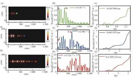
Fig. 7 (a, d, g) Screenshots of the electric field intensity distribution at t1, t2 and t3. (b, e, h) Cross-sectional electric field diagrams at the Zigzag boundary at different time t. (c, f, j) The changing process of the electric field at the capture point of light energy圖7 (a, d, g) t1,t2 和t3 時刻電場強度分布截圖。(b, e, h) 不同t 時刻Zigzag 邊界處截面電場圖。(c, f, j) 光能捕獲點處電場變化過程
4 Conclusion
In this paper, the time crystal band gap is periodically opened and closed by dynamically controlling the periodic change of the external voltage of the graphene nanodisk with time. Slow light transmission with the group velocity near zero is realized by the slow light waveguide made of graphene plasmon time crystal. The simulation results show that when the light propagates in the waveguide, a group velocity close to zero can be obtained, which is accompanied by the appearance of the field enhancement effect at the corresponding optical energy trapping point of the waveguide. In the case of adjusting the external bias voltage, the operating frequency of the slow optical waveguide can be effectively adjusted. Our research will be applied in the future to devices in the fields of on-chip light buffering and enhanced light-matter interactions.
——中文對照版——
1 引 言
慢光技術在光場調(diào)控及光存儲器件中的潛在應用前景頗為廣闊[1-3],因而備受關注。通過控制結構色散來實現(xiàn)慢光是目前常用的技術之一,該技術的主要方法是通過設計特定結構的慢光波導實現(xiàn)對光群速度的控制。已經(jīng)在多個研究中觀察到這類光子晶體波導中產(chǎn)生的慢光[4-5]。然而,在以往的慢光波導結構中,當群速度變慢,其支持的帶寬將變得非常狹窄,同時還伴隨著巨大的群速度色散效應。Scheuer J 等人采用結構復雜的耦合諧振光波導實現(xiàn)內(nèi)部色散補償,解決了失真問題[6]。近年來,人們采用表面等離激元極化子(Surface Plasmon Polaritons, SPPs)波導來實現(xiàn)慢光,在結構固定的情況下可以獲得更高的慢光容量,但慢光性能的調(diào)整受到限制[7]。同樣地,啁啾結構所具有的極大的群速度色散效應會使光信號嚴重失真,并且器件的工作頻率范圍有限[8]。再者,傳統(tǒng)的慢光器件的結構設計復雜且結構一旦固定其可調(diào)諧性能就很差,從而限制了它們的實際應用。
光子晶體擁有良好的拓撲能帶效應,其拓撲概念在光子學領域的應用中極具潛力,從而引起了人們的廣泛關注。拓撲光子結構已經(jīng)顛覆了一些關于波傳播和操控的傳統(tǒng)觀點。將拓撲光子晶體應用于波的傳播,可以實現(xiàn)如無反射的急劇彎曲的波、魯棒的延遲線、自旋極化開關和非互易器件[9],使新型的光子器件成為可能。最近,陳曉東等人提出并證明了拓撲光子晶體中的谷態(tài)可以作為拓撲保護來實現(xiàn)光的傳輸,該設計是將兩個拓撲結構不同的拓撲光子晶體鏡像放置構成可以實現(xiàn)拓撲保護的界面[10]。之后, Yoshimi 等研究人員提出了一種在谷態(tài)光子晶體中實現(xiàn)拓撲慢光波導的結構[11]。該波導結構是基于半導體基底,實現(xiàn)拓撲帶隙范圍內(nèi)群指數(shù)大于100 的慢光傳輸,但制作工藝較為復雜,不具備可調(diào)諧性,同時沒有涉及慢光所帶來的場強變化。隨著研究的深入,發(fā)現(xiàn)在折射率隨時間周期性變化的光子時間晶體材料中可以實現(xiàn)谷態(tài)這種拓撲帶隙結構[12]。方法是通過打破晶體時間平移對稱,光子時間晶體可以實現(xiàn)拓撲非平庸相位[13-15],從而影響光在晶體中的傳播。
眾所周知,石墨烯具有獨特的電學和光學特性,尤其是其支持表面等離子激元波,具有相對較低的歐姆損耗及較強的可調(diào)諧性等優(yōu)點[16]。Jin 等人設計了具有周期性圖案的單層石墨烯,通過引入靜態(tài)磁場實現(xiàn)了拓撲單向邊界傳輸[17]。之后,王洋等學者實現(xiàn)了用于傳感應用的雙層石墨烯超表面中的拓撲谷等離子體傳輸[18]。最近,郭翔等研究人員通過光子晶體線缺陷設計了石墨烯SPP 等效二維光子晶體慢光波導,通過石墨烯在空間上的化學勢漸變來實現(xiàn)慢光的調(diào)制[19]。同樣地,在時間上實現(xiàn)對石墨烯等離激元晶體谷態(tài)拓撲慢光傳輸?shù)恼{(diào)制是非常有意義的工作。本文提出了一種在石墨烯等離激元時間晶體構造的波導中實現(xiàn)拓撲慢光傳輸?shù)男路椒ā6S石墨烯等離激元時間晶體由一組呈蜂窩狀周期性排列的石墨烯納米盤組成。通過控制石墨烯的化學勢隨時間周期性變化,打破了石墨烯等離激元時間晶體的時間平移對稱性。數(shù)值仿真表明,等離激元時間晶體能帶帶隙可以隨時間周期性地打開和閉合。進一步研究發(fā)現(xiàn):鋸齒形邊可以支持在拓撲帶隙內(nèi)實現(xiàn)接近零的電磁傳輸群速度。對慢光波導電磁傳輸進行數(shù)值仿真,模擬結果表明該拓撲波導能夠產(chǎn)生慢光。該方法的優(yōu)點是結構簡單,具有較好的場增強效果和動態(tài)調(diào)諧能力,為動態(tài)實現(xiàn)光場調(diào)控提供了新的途徑和方法。
2 數(shù)值仿真方法和模型
本文基于石墨烯等離激元時間晶體實現(xiàn)谷態(tài)拓撲慢光傳輸波導。如圖1(a)(彩圖見期刊電子版)所示,該波導采用Zigzag 結構拓撲界面作為傳輸通道,頂部由石墨烯納米盤構成。石墨烯與空氣接觸,背景材料選擇的是SiO2,襯底材料是Si。從圖中的波導截面圖可以看出,偏置電壓加在石墨烯納米盤與硅襯底上。其中硅柱按三角晶格排列,V1(t),V2(t) 和V3(t) 分別是外加在石墨烯納米盤上的偏置電壓,這種方式是基于石墨烯等離激元的光子晶體機理實現(xiàn)的[20]。當石墨烯與襯底之間的距離一定時,通過改變外加電壓就可以改變石墨烯的化學勢。
假設石墨烯周圍環(huán)境的相對介電常數(shù)分別為 εr1和 εr2。其 中,襯底采 用相對 介電常數(shù) 為εr1=3.9 的SiO2,石墨烯上表面空氣的相對介電常數(shù)為 εr2=1。在該模型中,數(shù)值仿真考慮TM 模式,假設該TM 模式的電場形式為[21]:
將式(1)代入麥克斯韋方程組,通過添加石墨烯的表面電導率 (σg)參與公式變換,并匹配相應的邊界條件,得到TM 模式的色散關系[22]:
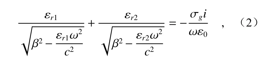
其中 ε0為自由空間中的真空介電常數(shù), ω為等離激元的角頻率,c為光在真空的傳播速度。在整個計算過程中,只考慮傳播常數(shù) β ?的情況,因此方程(2)簡化為以下形式[23]:
其中 β是基于石墨烯SPP 的傳播常數(shù),石墨烯的表面電導率 σg可隨溫度T、化學勢 μc,散射速率τ和 角頻率 ω進 行調(diào)節(jié),其由帶內(nèi)電子散射σintra和帶間電子躍遷 σinter兩個部分組成,根據(jù)Kubo公式[23]:
其中 kB是 玻爾茲曼常數(shù), e 是 電子的電荷,hˉ是約化普朗克常數(shù)。具體來說,石墨烯的化學勢 μc可以通過外部外加電壓有效地調(diào)節(jié)[20-21,24-25]。
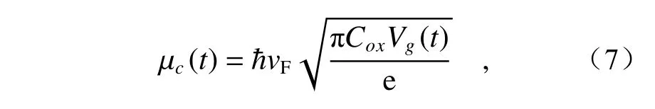
式中vF為費米速度,Cox為柵電容[26],Vg(t)為隨時間周期性變化的外加電壓。石墨烯納米盤外加偏置電壓隨時間周期性變化的曲線,如圖1(b)(彩圖見期刊電子版)所示。通過改變外加在石墨烯納米盤上的偏置電壓V1(t),V2(t) 和V3(t),可以改變石墨烯化學勢μc1(t), μc2(t)和 μc3(t)。
3 數(shù)值仿真結果與討論
3.1 石墨烯等離激元時間晶體模型及性能
首先,探究了由排列成三角晶格的石墨烯納米盤陣列組成的二維石墨烯等離激元晶體能帶拓撲結構。如圖2(a)所示,石墨烯等離激元時間晶體結構,虛線區(qū)域為晶體元胞,實線部分為晶體的布里淵區(qū),其中 Γ-M-K-Γ為簡約布里淵區(qū),a 是晶體晶格常數(shù),石墨烯納米盤半徑表示為r。μc1, μc2和 μc3分別是不同石墨烯納米盤的化學勢,由式(7)可知,這些石墨烯納米盤的化學勢也是可以隨時間作周期性變化的,固可以寫成 μc1(t),μc2(t)和 μc3(t)[27-29]。通過對石墨烯納米盤的外加偏置電壓加以V1(t),V2(t)和V3(t)的周期變化,可以在時間上靈活地控制其化學勢。在這里,計算了一個周期內(nèi)若干時刻石墨烯等離激元時間晶體的能帶,如圖2(b)(彩圖見期刊電子版)所示。其中,黑線描繪的是當t=0 s (即 Δμc=μc1-μc2=0 eV)時,石墨烯納米盤的化學勢分別為 μc1= μc2=0.3 eV 和μc3=0.6 eV,兩條能帶在K點處簡并相交于狄拉克點,且明顯不存在帶隙。在化學勢隨時間周期性變化的過程中,石墨烯等離激元時間晶體的時間平移對稱性被打破,狄拉克錐色散將被分裂,帶隙將會打開[30]。圖2(b)中的綠色、藍色和紅色曲線分別描繪了如下3 個時間節(jié)點的能帶結構:t1=1 e-12s (即 Δμc= 0.1 eV),t2= 1.5 e-12s (即 Δμc=0.12 eV)和t3= 2 e-12s (即 Δμc=0.14 eV)。很明顯,晶體能帶帶隙隨著時間的推移會經(jīng)歷一個從閉合到打開的過程。在這里值得注意的是,這種石墨烯等離激元時間晶體能帶隨時間的變化是可以在不改變幾何結構的情況下進行的。
為了驗證石墨烯等離激元時間晶體所具有的特性,本項工作設計了數(shù)值仿真實驗。如圖3(d)所示,在一片由石墨烯等離激元時間晶體構成的區(qū)域中,將一激勵源放置在P 點處,石墨烯納米盤的化學勢之間的關系 Δμc滿足圖3(a)中的變化規(guī)律。在這里,從激發(fā)源中激發(fā)出頻率為46.50 THz的電磁波。進一步探究在石墨烯化學勢變化的同時,時間晶體能帶帶隙的變化趨勢。通過分析帶隙的打開及關閉,當激發(fā)波的頻率位于導帶時,傳播現(xiàn)象發(fā)生;可當這個頻率處在帶隙內(nèi)時,波就不會在這個時間間隔內(nèi)傳播[31-33]。仿真結果如圖3(彩圖見期刊電子版) 所示,對傳輸過程中4 個時間節(jié)點的電場進行截圖。隨著 Δμc在時間上作周期性變化,分別在tb= 3.20 e-12s,tc=4.16 e-12s,td=5.82 e-12s和tf=8.24 e-12s 的時序中出現(xiàn)傳輸和禁止交替現(xiàn)象。而這個結果可以很好地說明,石墨烯等離激元時間晶體通過對化學勢進行周期性調(diào)控,可以實現(xiàn)能帶帶隙隨時間周期性的打開和關閉。
3.2 Zigzag 拓撲邊界結構理論與模型
當石墨烯等離激元時間晶體的時間平移對稱性被破壞時,狄拉克錐色散就不會受到保護。從群論的角度來看,當反轉對稱被打破時(K或K′)點的群對稱性會由C3v降為C3。在能帶上的表現(xiàn)為狄拉克錐遭到破壞,原本簡并于K點的兩條能帶將被打開[34-35]。能帶打開之后,有關能帶能谷處的軌道角動量出現(xiàn)變化,通過分析得到 了 在t1= 1 e-12s (即 Δμc= 0.1 eV),t2=1.5 e-12s (即Δμc= 0.12 eV)和t3= 2 e-12s (即 Δμc=0.14 eV)時刻K點的相位分布。如圖4(彩圖見期刊電子版)所示,可以看到在不同時刻兩條能帶簡并在K點分別出現(xiàn)了左旋圓極化(Left-handed Circular Polarized, LCP)和右旋圓極化(Right-handed Circular Polarized, RCP)的相位分布。也就是說,在 Δμc隨著時間變化的過程中,時間晶體能帶打開后任何時刻下的能谷都擁有方向相反的圓極化軌道角動量。因此,可以通過加載不同軌道角動量的電磁模來構成拓撲邊緣的電磁傳輸,這為利用拓撲邊界構造來構建慢光波導提供了理論基礎。
研究中采用Zigzag 拓撲邊界來構建慢光波導。這種拓撲結構是由石墨烯等離激元時間晶體構建的,它產(chǎn)生了“時間拓撲邊界態(tài)”,是拓撲邊緣態(tài)的時間模擬[13]。打破石墨烯等離激元時間晶體的時間平移對稱性會導致能帶簡并處的狄拉克點被打開,從而形成一個完整的帶隙,其中存在拓撲保護邊界模式。圖5(a)(彩圖見期刊電子版)中紅色虛線所在處為Zigzag 拓撲界面,通過對黑色虛線內(nèi)區(qū)域采樣,在商用仿真軟件COMSOL Multiphysics 中,建立有限周期(N=19) 的超胞單元模型。部分仿真結果如圖5(a)的底部所示,可以看出電場分布集中于邊界處。本文還計算了不同 Δμc時刻下該邊界模的色散關系(圖5(b)(彩圖見期刊電子版)),灰色區(qū)域表示投影的體能帶圖。圖5(b) 還描繪處出了t1= 1 e-12s,t2=1.5 e-12s和t3= 2 e-12s 3 個不同 Δμc時刻下的邊界態(tài)的投影能帶[36]。很顯然,當 Δμc隨時間變化時,在每個時刻上總有與之相應的邊界態(tài)存在,這就意味著實現(xiàn)了基于石墨烯等離激元時間晶體Zigzag 拓撲邊界態(tài)的時間模擬。
3.3 慢光現(xiàn)象和場增強效應
進一步分析上述邊界模的色散關系,可以推出在色散曲線的極值點存在群速度為零(慢光)的現(xiàn)象。為了更好地研究存在于該邊界態(tài)中導模的群速度,將3 個不同時刻的部分色散曲線繪制于圖6(a)(彩圖見期刊電子版)中,很明顯,伴隨著嚴重彎曲的色散,因此導致間隙內(nèi)慢光模式的存在。根據(jù)這些邊界模的色散曲線,由角頻率 ω與群速度vg關 系滿足vg=dω/dk[37-38],可以計算出群速度隨頻率的變化曲線。如圖6(b)(彩圖見期刊電子版) 所示,紅色曲線是在t1= 1 e-12s 時刻 Δμc=0.1 eV 時的群速度,群速度趨近于零,頻率趨于50.237 0 THz。當在t2= 1.5 e-12s 時刻, Δμc=0.12 eV時,電磁波群速度在50.114 9 THz頻率處接近于零,以藍色曲線描繪在圖6(b)中。而在t3=2 e-12s時刻 Δμc=0.14 eV 時,在頻率為49.929 2 THz,群速度接近零,由綠色曲線標出。數(shù)值計算結果表明,不同頻率的電磁波會在不同時間達到零群速度。也就是說,該拓撲邊界可以實現(xiàn)在不同時刻支持某一頻率電磁波群速度接近零的慢光。
最后,根據(jù)圖1(a)中所給出的慢光波導模型,在仿真軟件COMSOL 中對其進行二維建模,設計采用Zigzag 邊界結構作為傳輸通道,激勵源位于P處(如圖1(a) 所示)。對石墨烯納米盤的外加偏置電壓加以V1(t),V2(t) 和V3(t) 的周期變化,可以在時間上靈活地控制其化學勢。將一定頻率的石墨烯SPP 波由P點處發(fā)出,可以得到其在波導中隨時間傳輸?shù)恼麄€過程。圖7(彩圖見期刊電子版)給出的是頻率分別為50.237 0 THz、50.114 7 THz 和49.929 2 THz的平面波在波導中傳輸?shù)碾妶鰪姸确植冀Y果。在本次模擬仿真中,取頻率為50.237 0 THz 的平面波從t0=0 s 時刻由P點處持續(xù)性激勵,沿波導傳輸1 e-12s后達到群速度接近零的狀態(tài),該SPP波傳輸停滯在X=307.998 nm 位置處。圖7(a)(彩圖見期刊電子版)所示是頻率為50.237 0 THz 的平面波在t1=1 e-12s 時刻的電場截圖。在平面波群速度接近零后繼續(xù)保持慢光模式下的持續(xù)激勵,結果發(fā)現(xiàn)X=307.998 nm 位置處(圖7(a)中綠點)的電場強度在t=1.4 e-12s 時刻達到了最大值,且此時的電場強度遠大于激勵源處的電場強度。將t=1.4 e-12s時刻波導中的電場強度描繪在圖7(b)中,可以發(fā)現(xiàn)此時光能捕獲點處的場強B大于激勵源處的場強A。將t0=0 s 至t=1.4 e-12s 時間段內(nèi)在綠點位置處電場強度變化過程描繪在圖7(c)中。可以看到,由于慢光傳輸中的場增強效應,波導在光能捕獲點(綠點)處實現(xiàn)了電場強度的持續(xù)疊加并高于激勵源的增強效果[4]。圖7(d)展示了頻率為50.114 7 THz 的SPP波從t0=0 s 時刻由P點處持續(xù)性激勵,沿波導傳輸時間1 .5 e-12s后的電場分布圖。SPPs 波傳輸來到t2=1.5 e-12s 時刻,在X=667.879 nm 位置處的群速度下降至零。同時還對光能捕獲點X=667.879 nm 處(圖7(d) 中藍點) 的電場進行了持續(xù)觀測,得到t=2.98 e-12s時刻的邊界處電場分布截面圖,如圖7(e) 所示。該結果表明,在t=2.98 e-12s 時刻光能捕獲點處的電場強度達到最大值D,并且大于P點處的電場強度C。圖7(f)描繪了從時間t0=0 s 到t=2.98 e-12s,藍點處的電場強度疊加過程。同理,如圖7(g) 所示,頻率為49.929 2 THz 的SPP 波從t0=0 s 時刻由P點處不斷的激勵,沿波導傳輸 2 e-12s后達到接近零的群速度,波導對于該SPP 波傳輸?shù)墓饽懿东@位于X=1 029.122 nm 處(圖7(g)中紅點)。在保持慢光模式下進行持續(xù)性激勵,觀測發(fā)現(xiàn)光能捕獲處的電場在t=3.22 e-12s 時刻到達最大強度F,該電場強度遠大于激勵源處的電場強度E,如圖7(j)所示。從t0=0 s 至t=3.22 e-12s 時間段內(nèi)在紅點位置處電場強度變化過程描繪在圖7(j)中,同樣經(jīng)歷了一個場強疊加的過程。上述模擬仿真過程取了3 個頻率的SPP 波,分別在改變石墨烯納米盤外加偏置電壓將光群速度調(diào)制接近零。在場增強效應的影響下,波導在光能捕獲點處實現(xiàn)了電場強度持續(xù)疊加并高于激勵源處的電場強度。這些結果表明,該慢光波導可以實現(xiàn)不同頻率的SPP 波在不同的時間和位置處停滯下來,并在相應的光能捕獲點處發(fā)生場增強效應。在這項工作中使用石墨烯等離激元時間晶體構造傳輸波導,僅通過調(diào)諧石墨烯化學勢就可以實現(xiàn)對慢光群速度的調(diào)制。其與光子晶體線缺陷波導[19]等傳統(tǒng)波導相比,在結構上更為簡單,即使結構固定,也可以通過改變外加電壓靈活調(diào)制波導性能,極大地提高了慢光波導的電可調(diào)諧性。此外,SPP 波在該拓撲邊界傳輸表現(xiàn)為電場幅值不斷衰減的倏逝波,傳輸距離愈遠衰減愈強。在激勵源處施加持續(xù)的激勵,通過記錄波導光能捕獲點處的場強疊加過程,在時間上直觀地展現(xiàn)了由場強疊加效應所引起的電場變化,是之前對慢光研究工作中所沒有的[11]。由于波導中的模式并非是離散的,會發(fā)生前后向模式的簡并,最終使能量流失。因而在時序中實現(xiàn)光群速度為零時,所謂“靜止彩虹”的完全停止光群速度的現(xiàn)象并不會真實發(fā)生。
4 結 論
本文通過動態(tài)控制石墨烯納米盤外接電壓隨時間的周期性變化,使時間晶體的能帶帶隙周期性地打開和關閉。利用石墨烯等離激元時間晶體制作慢光波導,獲得了群速度接近零的慢光傳輸。仿真結果表明,光在該波導中傳播時,可以獲得接近零的群速度,并伴隨著相應的波導光能捕獲點處場增強效應的出現(xiàn)。在調(diào)節(jié)外部偏置電壓的情況下,慢光波導的工作頻率可以得到有效的調(diào)節(jié)。本項研究將在未來應用于片上光緩沖和增強光與物質的相互作用領域的器件中。