A 4×4 metal-semiconductor-metal rectangular deep-ultraviolet detector array of Ga2O3 photoconductor with high photo response
2022-08-31 10:00:02ZengLiu劉增YuSongZhi支鈺崧MaoLinZhang張茂林LiLiYang楊莉莉ShanLi李山ZuYongYan晏祖勇ShaoHuiZhang張少輝DaoYouGuo郭道友PeiGangLi李培剛YuFengGuo郭宇鋒andWeiHuaTang唐為華
Chinese Physics B 2022年8期
Zeng Liu(劉增) Yu-Song Zhi(支鈺崧) Mao-Lin Zhang(張茂林) Li-Li Yang(楊莉莉)Shan Li(李山) Zu-Yong Yan(晏祖勇) Shao-Hui Zhang(張少輝) Dao-You Guo(郭道友)Pei-Gang Li(李培剛) Yu-Feng Guo(郭宇鋒) and Wei-Hua Tang(唐為華)
1College of Integrated Circuit Science and Engineering,Nanjing University of Posts and Telecommunications,Nanjing 210023,China
2National and Local Joint Engineering Laboratory for RF Integration and Micro-Packing Technologies,Nanjing University of Posts and Telecommunications,Nanjing 210023,China
3China Academy of Launch Vehicle Technology,Beijing 100076,China
4School of Science,Beijing University of Posts and Telecommunications,Beijing 100876,China
5Institute of Microscale Optoelectronics,Shenzhen University,Shenzhen 518060,China
6Center for Optoelectronics Materials and Devices,Department of Physics,Zhejiang Sci-Tech University,Hangzhou 310018,China
Keywords: Ga2O3,array photodetector,MOCVD,deep UV detection
1. Introduction
Wide and ultra-wide bandgap (Eg) semiconductor ultraviolet (UV) photodetectors, owing to their preferable natural properties,[1,2]cater for the desired demands of optical communications, short-distance communications, medical imaging,safety monitoring,environmental protection,and life sciences, etc.[3–8]Among the various wideEgsemiconductors,gallium oxide (Ga2O3) has theEgof around 4.8 eV,[9,10]exactly translating to the precise deep-ultraviolet (UV) photo detection,[11–15]along with low false alarming rate. As far as it goes,the Ga2O3-based deep-UV photodetectors are constructed in the forms of metal-semiconductor-metal (MSM)structures,[16–18]p–n junctions,[19–21]organic–inorganic hybrid heterojunctions,[22–24]Schottky photodiodes,[25–29]fieldeffect phototransistors,[30–33]and nanorod/nanowire array heterojunction,[34]etc. Such devices have shown excellent optoelectronic performances and provided a promised potential for further developing Ga2O3-based deep-UV photodetectors.While, these photodetectors are mainly focused on the study of the cell device, in spite of great breakthroughs. For actual applications in imagers,the uniformly high-performance photodetector array is seriously desired.[35–37]
In this respect,Penget al.[38]reported the 32×32,16×16,8×8, and 4×4 photodetector arrays with sputtering Ga2O3films,in which the 4×4 Ga2O3photodetector array displayed a photo responsivity(R)of 0.89 A·W?1and an external quantum efficiency(EQE)of 444%at 250 nm UV light irradiation,along with a deviation of 12.1% forR. Pratiyushet al.[39]displayed a floze-zone grown Ga2O31×8 photodetector array of 4 A·W?1at 40 V, while it had a large deviation of 62%for dark current (Idark). In addition, Zhiet al.[40]published a work that a Ga2O316×4 linear array has shown a highRof 139.56 A·W?1with a deviation of 10%. What’s more, Chenet al.[41]and Qinet al.[42]inhabited the deep-UV imaging application by right of Ga2O3photodetector array. The further development is urgently desired for highRand decent deviations. Therefore, a high-performance photodetector array is fabricated and discussed in this paper.
2. Experimental details
In this work, we use the metalorganic chemical vapor deposition (MOCVD) to deposit the Ga2O3thin film, and then construct the photodetector array through photolithography, lift-off,and ion beam sputtering techniques. The Ga2O3thin film are characterized by x-ray diffraction (XRD) and atomic force microscope(AFM).The electrical and optoelectrical properties including current–voltage (I–V) and timedependent current(I–t)are measured by a Keithley 4200 semiconductor analysis meter in air at the room temperature. The UV light source is a UV lamp that could emit 254 nm and 365 nm UV light, and the light intensity could be tuned by changing the distance between the photodetector and lamp.
Concretely, the Ga2O3thin film was grew on the sapphire substrate by using MOCVD at temperature of 735?C and chamber pressure of 25 Torr with the [O/Ga] molar ratio of about 1650.[16]Triethylgallium(TEGa)and oxygen are used as the Ga and O sources,and TEGa is kept at temperature of 35?C and chamber pressure of 760 Torr. Further detailed growth could be seen in Ref. [43]. XRD and AFM are used to characterize the crystal quality of the prepared film,such as the diffraction peaks and root mean square(RMS)roughness.
By photolithography, lift-off, and ion beam sputtering, a Ga2O3photodetector array is fabricated as shown in Fig. 1.The symmetrical Ti/Au interdigital metal electrodes are patterned on the surface of the Ga2O3thin film. The fabricated photodetector array is annealed in N2at 200?C for 60 s, for achieving good Ohmic contacts, in which the electrical and optoelectrical properties is like a photo sensitive conductor.Every photodetector cell is 10 fingers metal-semiconductormetal(MSM)structure. As shown in Fig.1, the device scale is 5 μm wide, 190 μm long, and 5 μm spacing distance. As calculated, the effective illuminated area (S) of one photodetector cell is 18450 μm2. At last, the current–voltage (I–V)and time-dependent current (I–t) performances are measured by employing the Keithley 4200, in order to exam the optoelectrical performances of the prepared photodetector array.
3. Results and discussion
As shown in Fig.2(a),the XRD pattern of the MOCVDgrown Ga2O3thin film is provided,indicating the(ˉ201),(ˉ402),and (ˉ603) diffraction peaks forβ-Ga2O3existence. In addition,the other peaks in the XRD pattern are from the sapphire we used for Ga2O3deposition. In Fig. 2(b), the AFM image of the MOCVD-grown (ˉ201)-orientedβ-Ga2O3thin film is shown,suggesting RMS roughness of 6.21 nm,and the AFM scanning area is 10×10μm2.
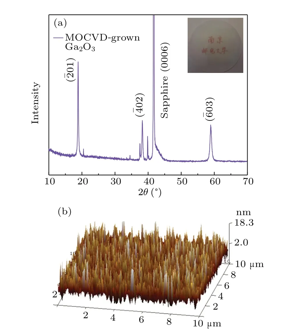
Fig.2.(a)The XRD pattern,and(b)AFM image of the MOCVD-grown Ga2O3 thin film.
With the aforementioned Ga2O3thin film characterized in Fig. 2, the photodetector array is fabricated. The energyband diagram of one photodetector cell is shown in Fig. 3.Corresponding to the electron affinity of Ga2O3[χ(Ga2O3)~4.0 eV] and work function of Ti [Φ(Ti)~4.33 eV], the interfacial barrier at Ti–Ga2O3interface (??Ti?Ga2O3) is about 0.33 eV. Such a small barrier could guarantee the nearly-Ohmic contact in this device.
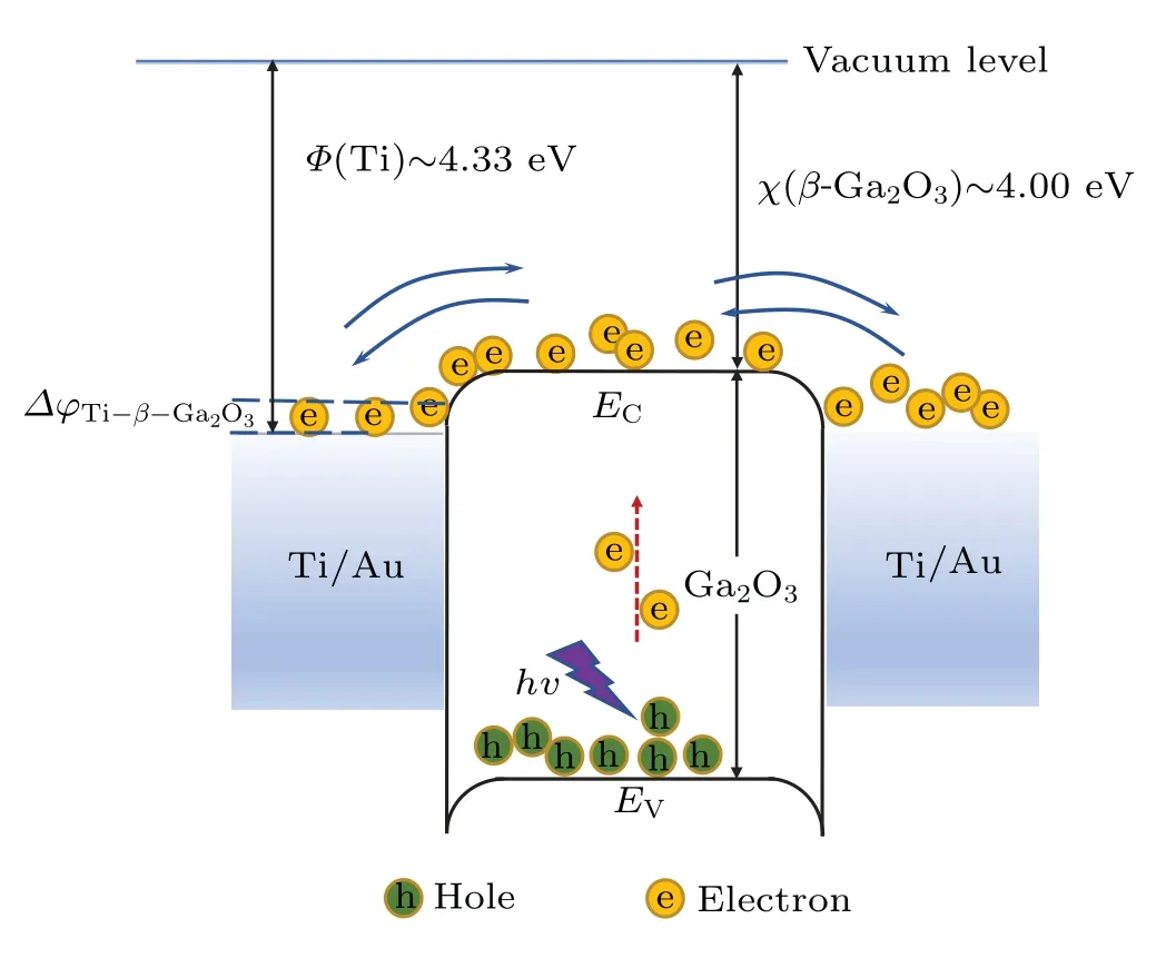
Fig.3. The energy-band diagram of the photodetector cell.
Correspondingly,in Fig.4(a),for one photodetector cell,theI–Vcurves in the dark and under illuminations are expressed,all suggesting sub-Ohmic contacts,on account of the small metal–semiconductor interfacial barrier of Ti–Ga2O3according to the Schottky–Mott rule.[44–46]The dark current (Idark) is about 1.94×10?12A at bias of 10 V, and the photocurrent (Iphoto) is 6.43×10?5A, 7.59×10?5A,8.23×10?5A, 1.02×10?4A, 1.17×10?4A, 1.54×10?4A,and 1.74×10?4A under illuminations with light intensity of 400μW·cm?2,500μW·cm?2,600μW·cm?2,800μW·cm?2,1000 μW·cm?2, 1500 μW·cm?2, and 2000 μW·cm?2, respectively. Correspondingly, the photo-to-dark current ratio (PDCR) is 3.31×10⁷, 3.91×10⁷, 4.24×10⁷, 5.25×107,6.0×107,7.94×107,and 8.97×10⁷,indicating high photo response to 254 nm UV light irradiation. For a photodetector,theR, specific detectivity (D?), EQE, and linear dynamic region(LDR)are always used to characterize the photodetector performances. They are expressed as follows:[47–49]
withPas the light intensity,Sas the effective irradiated area of the photodetector,eas the electron charge,has the Planck’s constant,cas the light speed, andλas the wavelength(254 nm).
At bias of 10 V and illuminated intensity of 1000μW·cm?2,theRis calculated to be 634.15 A·W?1,suggesting high photo response of the fabricated photodetector,and lots of electron-hole pairs are photoexcited owing to the highly reaction between the incident photons and the Ga2O3matter.[50,51]TheD?is 5.93×1011cm·Hz1/2·W?1(Jones),leading to a decent signal/noise performance, where theIdarkis considered as the main noise.[48]The EQE is as high as 310000%, and the photodetector cell is well-coupled to the incident 254 nm deep-UV light. In addition, the LDR is 108.94 dB.Without using the constraint of carriers in heterojunctions and Schottky junctions,[22,24,26–28]the MSM photodetector here is superior to the most similar devices.[11,12]On account of two issues: 1) the uniformity of semiconductor and 2) the potential difference caused by electrodes, the charge density and the band diagram are associated with a negatively charged semiconductor surface both in the dark and under illuminations. The presence of a high density of surface bound states for electrons(majority carrier in Ga2O3)is lying inside the bandgap,and is closing to Fermi level(i.e.,the Fermi pinning effect). Therefore, the time evolution of the surface space charge region could be assumed as Schottky diode, as though under open-circuit conditions.[50]The gain(G),defined as the increase of collected carriers per absorbed photon, for this photoconductor is mainly from the so-called metal–semiconductor diode, as shown in Fig. 3. The photoconductiveGcan be expressed as
where ?Iis the measured current difference between the conditions of both in the dark and under illuminations, andhνis the incident photon energy. So, theGcan be obtained as 41.01 dB.
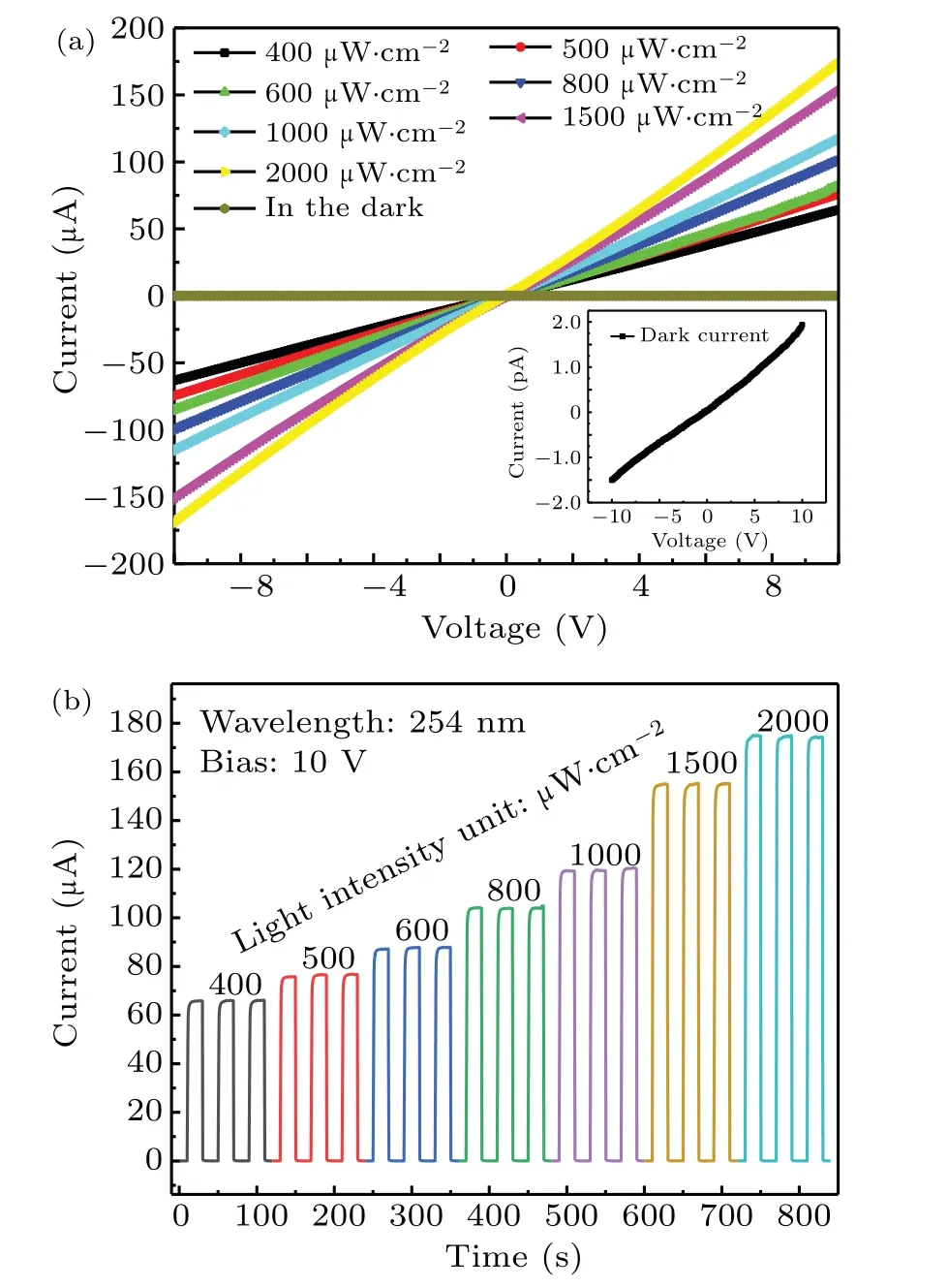
Fig. 4. For the photodetector cell. (a) The current–voltage curves under illuminations with different light intensities from 400 μW·cm?2 to 2000 μW·cm?2 at bias from ?10 V to 10 V. (b) The timedependent current under illuminations with different light intensities from 400μW·cm?2 to 2000μW·cm?2 at bias of 10 V.

Fig.5. The light intensity-dependent photocurrent of the photodetector cell.
In Fig. 4(b), theI–tperformances of the photodetector cell under illuminations with different light intensities are shown. Higher light intensity contributes to higherIphoto. Under various light intensity irradiations, the photodetector cell displays stable and repeatable cycling opto-switching behaviors. As shown in Fig. 5, theIphotodisplays good linear relationship with the light intensity, indicating that the photodetector may well operate in a linear dynamic region.
Figure 6 displays theIphotoandRof the 16 photodetector cells. The deviation ofRis estimated to be 19.6%on account of a relationship of[(Rmax?Rave)/Rave],[39]withRmaxas the maximumR, andRaveas the averageRfor the 16 photodetector cells. It is worthy to be noted that the deviation ofRis relatively large. It may well be due to the large RMS of the Ga2O3film used for fabricating photodetector array. The photodetectors with films of different thicknesses have different performances,[52]leading to the highRdeviation of photodetector array. In addition, the difference of electrode line configuration in all the cells could be another cause for having large deviation. What’s more, theIphotoandRseem a regular evolution, and we found that the photodetector cells around the photodetector array have higherIphotoandR,while the photodetector cells in the center area have relatively lowIphotoandR. The photodetector cells in the center area always have long pathway for carrier transports,in which a relatively high resistance leads to a low outputIphoto, thus a lowR. To some degree,it also decreases the uniform performance of the photodetector array. In all, beyond the study on the cell photodetector,photodetector array is urgently desired for high performances and better uniformity.
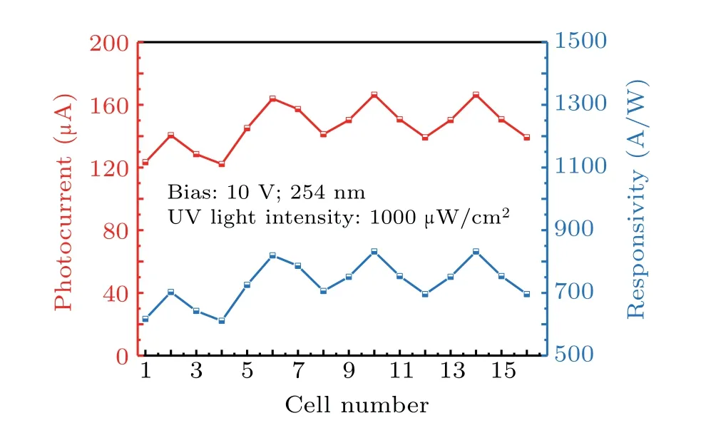
Fig. 6. Photocurrents and photo responsivities of the 16 Ga2O3 deep-UV photodetectors at 10 V bias and under illumination with intensity of 1000μW/cm2.
4. Conclusion
In summary, a 4×4 rectangular photodetector array is introduced based on MOCVD-grownβ-Ga2O3thin film.The photodetector cell displaysRof 634.15 A·W?1,D?of 5.93×10¹¹Jones, EQE of 310000%, and LDR of 108.94 dB at bias of 10 V and under illumination with light intensity of 1000μW·cm?2,indicating high optoelectronic performances of the fabricated device.And the photoconductiveGis 41.01 dB.For the photodetector array with 16 cells,the deviation ofRis 19.6%. The good performances of the photodetector described here is owing to the high-qualityβ-Ga2O3thin film and the successful construction of the array. This work may well provide a promised route for developing the deep-UV photodetection by using Ga2O3.
Acknowledgements
Project supported by the National Natural Science Foundation of China (Grant No. 61774019) and Natural Science Research Start-up Foundation of Recruiting Talents of Nanjing University of Posts and Telecommunications (Grant Nos.XK1060921115 and XK1060921002).
- Chinese Physics B的其它文章
- Magnetic properties of oxides and silicon single crystals
- Non-universal Fermi polaron in quasi two-dimensional quantum gases
- Purification in entanglement distribution with deep quantum neural network
- New insight into the mechanism of DNA polymerase I revealed by single-molecule FRET studies of Klenow fragment
- Wake-up effect in Hf0.4Zr0.6O2 ferroelectric thin-film capacitors under a cycling electric field
- Characterization of topological phase of superlattices in superconducting circuits