Moir′e superlattice modulations in single-unit-cell FeTe films grown on NbSe2 single crystals?
2021-12-22 06:44:50HanBinDeng鄧翰賓YuanLi李淵ZiliFeng馮子力JianYuGuan關劍宇XinYu于鑫XiongHuang黃雄RuiZheLiu劉睿哲ChangJiangZhu朱長江LiminLiu劉立民YingKaiSun孫英開XiLiangPeng彭錫亮ShuaiShuaiLi李帥帥XinDu杜鑫ZhengWang王錚RuiWu武睿JiaXinYin殷嘉鑫YouGuoShi石友國a
Chinese Physics B 2021年12期
Han-Bin Deng(鄧翰賓) Yuan Li(李淵) Zili Feng(馮子力) Jian-Yu Guan(關劍宇)Xin Yu(于鑫) Xiong Huang(黃雄) Rui-Zhe Liu(劉睿哲) Chang-Jiang Zhu(朱長江)Limin Liu(劉立民) Ying-Kai Sun(孫英開) Xi-Liang Peng(彭錫亮) Shuai-Shuai Li(李帥帥)Xin Du(杜鑫) Zheng Wang(王錚) Rui Wu(武睿) Jia-Xin Yin(殷嘉鑫)You-Guo Shi(石友國) and Han-Qing Mao(毛寒青)
1Beijing National Laboratory for Condensed Matter Physics and Institute of Physics,Chinese Academy of Sciences,Beijing 100190,China
2School of Physics,University of Chinese Academy of Sciences,Beijing 100049,China
3Songshan Lake Materials Laboratory,Dongguan 523808,China
4Laboratory for Topological Quantum Matter and Spectroscopy(B7),Department of Physics,Princeton University,Princeton,NJ 08544,USA
5Center of Materials Science and Optoelectronics Engineering,University of Chinese Academy of Sciences,Beijing 100049,China
Keywords: scanning tunneling microscopy(STM),atomic force microscopy(AFM),FeTe film,moir′e superlattice,misorientation
1. Introduction
Interface engineering may lead to many exotic quantum phenomena. In recent years, topological superconductivity and Majorana fermions for fault-tolerant quantum computation have been found in fabricated interface systems with a topological insulator and a conventional s-wave superconductor.[1–8]On the other hand, fractal quantum Hall effect, unconventional superconductivity, and Mott insulator have been found in the fabricated interface system with moir′e superlattice which significantly modifies its electronic properties.[9–14]
Non-trivial topology has been proposed in Fe(Te,Se)single crystal and thin film.[5–18]While 2H-NbSe2single crystal is a prototype of conventional s-wave superconductor. If the two materials are used to fabricate the interface system,non-trivial topology and superconductivity may take place.[1,2]However, the two materials are in different crystallographic symmetries. Fabricating an atomically sharp interface between them is not an easy task and misorientation of different angles between them is expected. In addition,the different heights of Te atom and Se atom may hinder the STM/AFM investigation of the interface structure between Fe(Te,Se) film and NbSe2substrate. Therefore, FeTe film which has the same lattice structure but a simpler chemical composition may be an alternate. According to the DFT calculations of Wu,[17]single-unit-cell(1UC)FeTe becomes topological nontrivial whenaFeTe<3.905 ?A.Although the band topology of 1UC FeTe film grown on NbSe2(aFeTe≈3.9 ?A) is still not clear, it is wise to use 1UC FeTe/NbSe2as a prototype of 1UC Fe(Te,Se)/NbSe2to investigate their interface structure.Therefore,the influence of misorientation on the structural relaxation and/or electronic reconstruction of FeTe/NbSe2may be explored.
Here in this paper, we grow atomically flat 1UC FeTe film on 2H-NbSe2single crystal by a molecular beam epitaxy (MBE) system and investigate itin-situwith home-built STM/AFM.In the STM topographic image of the grown FeTe film,we find different stripe-like superlattice modulations associated with different misorientation angles with respect to the NbSe2substrate. By superimposing the tetragonal FeTe lattice on the hexagonal NbSe2lattice, we reproduce the key features of the stripe-like superlattice modulations. Therefore,our results show that the stripe-like superlattice modulations are moir′e superlattice modulations, indicating an atomically sharp interface between FeTe film and NbSe2substrate. Our results also suggest an electronic origin of the moir′e superlattice modulations in most of the cases when the misorientation angle is relatively small(≤3?),because we find that the moir′e superlattice modulations are absent in AFM topographic image. While when the misorientation angle is relatively large(≥10?), structural relaxation emerges with the larger periodicity of the moir′e superlattice modulations.
2. Methods
The 2H-NbSe2(001)substrates typically 2×2×0.5 mm in size are glued on a titanium holder with H20E from Epoxy Technology.The substrates are transferred into our home-built cryogenic STM–AFM–MBE combined system.[19]Then the substrates are cleaved in a vacuum after degassing at 320?C for at least 6 hours. So large, flat, and clean surfaces are achieved.
The 1UC FeTe(001)films are epitaxially grown on substrates with co-evaporation of high-purity Fe (99.98%) and Te (99.99%) from standard Knudsen cells for 6×12 minutes, while the substrates are heated to 260?C. The stable fluxes of Fe and Te sources are obtained by heating the cells to 1045?C and 300?C, respectively. The high-quality films are achieved by post-annealing at 260?C for~4 hours. After post-annealing,the FeTe films are quickly transferred to anin-situcryogenic STM/AFM for measurement.
Both STM and AFM measurements can be applied by our home-made cryogenic STM/AFM system. When using an STM tip holder,the traditional STM function can be realized.When using an AFM tip holder of qPlus configuration, amplitude modulated (AM) or frequency modulated (FM) AFM measurement can be realized. By an additional electrode connecting the metal tip of the qPlus sensor,the tunneling current can be picked up during AFM measurement simultaneously.Electrochemically etched tungsten tips are used in both STM and AFM modes,which arein-situmodified by gently touching the Ag(111)film surface.All STM topographic images are obtained in constant current mode at 4 K.The typicalQfactor of the qPlus sensor is~35000 at 4 K,with resonant frequency at about 25 kHz.
The step height of the 1UC FeTe film is~7.4 ?A, relatively larger than the step height of the second-unit-cell FeTe film,which is~6.3 ?A.
The misorientation angle?is measured by comparing FeTe lattice vectors with respect to NbSe2lattice vectors.Only one domain has been found in each NbSe2substrate. So the lattice vectors of NbSe2can either be measured before or after the film deposition.
3. Results and discussion
The 2H-NbSe2and FeTe are layered materials with different crystallographic symmetries,as shown in Fig.1(a). The unit cell of 2H-NbSe2consists of two hexagonal Nb layers.Each Nb layer is sandwiched by two hexagonal Se layers. The weakest bonding is the Van der Waals (VdW) interaction between adjacent Se layers, where cleavage takes place. While the unit cell of FeTe consists of one tetragonal Fe layer sandwiched by two tetragonal Te layers. The bonding between adjacent Te layers is also VdW interaction. Therefore,the bonding between FeTe film and NbSe2substrate is also expected to be weak. And misorientation of different angles may take place. As shown in Fig. 1(b), the misorientation angle?is defined as the minimum angle between FeTe lattice vectors(aTe?Te) with respect to NbSe2lattice vectors (aSe?Se). Most of the grains of the grown FeTe films have relatively small misorientation angles (? ≤3?). However, grains with misorientation angles between 3?to 15?have also been found.Figures 1(c)and 1(e)show two typical atomic-resolved STM topographic images of 1UC FeTe film,with the misorientation angle? ~0?and~15?, respectively. The lattice periodicity of the topmost Te layer is measured~3.9 ?A by the reciprocal vectors in their corresponding FFT images(indicated by the red arrows in Figs. 1(d) and 1(f)). Besides the lattice periodicity,nanoscale stripe-like superlattice modulations can also be resolved. Comparing Fig.1(c)with Fig.1(e),we find the stripe-like superlattice modulations are different when the misorientation angle varies. Figures 1(d) and 1(f) are their corresponding FFT images. When the misorientation angle?is~0?, three pairs of wave vectors(indicated by the red circles in Fig.1(d))show similarly strongest intensity. However,only one pair of wave vectors (indicated by the red circles in Fig. 1(f)) show the strongest intensity when the misorientation angle?is~15?. The variation of the stripe-like superlattice modulations when the misorientation angle?changes can also be found near the grain boundaries. Figure 1(g) is an atomic-resolved STM topographic image probed near a domain boundary. In its FFT image Fig. 1(h), two groups of reciprocal vectors can be resolved,as indicated by the two red arrows. We find that the misorientation angle?is~1.5?in the bottom-right domain and~10.5?in the top-left domain.In the bottom-right domain when?is small,the stripe-like superlattice modulations resemble the ones in Fig.1(c).While in the top-left domain when?is relatively larger,the stripe-like superlattice modulations look similar to the ones in Fig.1(e).The dependence of the stripe-like superlattice modulations on the misorientation angle?is consistent in our different samples,implying it is the intrinsic property of 1UC FeTe/NbSe2film.
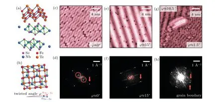
Fig. 1. (a) Illustration of 1UC FeTe film grown on NbSe2 single crystal. (b) Top view of 1UC FeTe film grown on NbSe2 single crystal. The misorientation angle ? is defined as the minimum angle of FeTe lattice vectors(aTe?Te)with respect to NbSe2 lattice vectors(aSe?Se). Only topmost Se–Nb–Se layers are plotted for simplicity. (c) An atomic-resolved STM image of 1UC FeTe film when the misorientation angle ? is ~0?. The junction setup is Vbias=100 mV,Iset=1.8 nA.(d)The FFT image of(c). The reciprocal vectors of the tetragonal Te layer and the strongest superlattice modulations are marked by red arrow and red circles,respectively.The periodicities of the three pairs of strongest superlattice modulations are ~13.6 ?A,~10.4 ?A,and ~10.2 ?A,respectively. (e)An atomic-resolved STM image of 1UC FeTe film when the misorientation angle ? is ~15?(the max value of misorientation angle between a tetragonal lattice and a hexagonal lattice). The junction setup is Vbias=100 mV,Iset=100 pA.(f)The FFT image of(e). The reciprocal vectors of the tetragonal Te layer and the strongest stripe-like superlattice are marked by red arrow and red circles,respectively. The periodicity of the pair of strongest superlattice modulation is ~31.7 ?A.(g)An atomic-resolved STM image of 1UC FeTe film near a domain boundary.The misorientation angles ? on two sides of the grain boundary are ~1.5?and ~10.5?,respectively. The junction setup is Vbias=10 mV,Iset=200 pA.(h)The FFT image of(g). The reciprocal vectors of tetragonal Te lattice on two sides of the grain boundaries are marked by the two red arrows.

Fig.2. (a)The simulated moir′e pattern between FeTe lattice and NbSe2 lattice in Fig.1(c). The misorientation angle ? is set to 0.5?. (b)The simulated moir′e pattern between FeTe lattice and NbSe2 lattice in Fig.1(e). The misorientation angle ? is set to 14.5?. (c)The simulated moir′e pattern between FeTe lattice and NbSe2 lattice near a grain boundary in Fig. 1(g). The misorientation angle ? in the bottom-right FeTe domain is set to 1.5?, and the misorientation angle ? in the top-left FeTe domain is set to 10.5?. The grain boundary is indicated by the thick white polyline in the graph.
Several previous reports have found stripe-like moir′e superlattice modulations in FeSe/Bi2Se3and FeSe/Pb interface systems.[20–25]Therefore, the stripe-like superlattice modulations found in FeTe/NbSe2film may also form by the moir′e pattern between film and substrate. By superimposing the tetragonal lattice of FeTe film (red circles) on the hexagonal lattice of NbSe2substrate (blue circles, here the CDW modulation in NbSe2is excluded for simplicity), we simulate the moir′e pattern between epitaxial FeTe films and NbSe2substrates.[20,26]The simulated moir′e patterns are shown in Figs. 2(a)–2(c), respectively. Comparing them with the measured STM topographic images, we find that the simulated moir′e patterns reproduce the periodicities and the directions of the stripe-like superlattice modulations in all the cases. Hence our simulation strongly supports that the stripe-like superlattice modulations found in 1UC FeTe/NbSe2films are also moir′e superlattice modulations, which are driven by the influence of the crystal field of the NbSe2substrate on the FeTe film.
The periodic crystal field of the NbSe2substrate may lead to structural relaxation or electronic reconstruction on the FeTe film. Since the noncontact AFM topographic image is less sensitive to the electronic structures than the STM topographic image,[27–29]it is beneficial to recheck the moir′e superlattice modulations with AFM measurement. Most of the FeTe grains have relatively small misorientation angles (? ≤3?)and their properties are similar. Figure 3(a)is an atomicresolved STM topographic image of the FeTe film when the misorientation angle?is~3?. Figure 3(b) is an AFM topographic image of the same field of view (FOV), in which the moir′e superlattice modulations can not be resolved. While in the simultaneously obtained current image from the tungsten tip,as shown in Fig.3(c),the moir′e superlattice modulations can still be resolved. In relatively rare cases,FeTe grains with larger angles can also be found. Figures 3(d)and 3(g)are atomic-resolved STM topographic images of FeTe film when the misorientation angles are~7?and~12?, respectively.Figures 3(e) and 3(h) are atomic-resolved AFM topographic images of the same FOVs,respectively. When the misorientation angle?is~7?,the moir′e pattern in the AFM topological image can hardly be resolved. While when the misorientation angle?is~12?, the moir′e pattern in the AFM topological image can be clearly resolved. In the simultaneously obtained current image from the tungsten tip,as shown in Figs.3(f)and 3(i), the moir′e superlattice modulations can also be resolved.Hence our STM–AFM combined results suggest an electronic origin of the moir′e superlattice modulations when the misorientation angle?is relatively small (≤3?) and structural relaxation emerges when the misorientation angle?is relatively large(≥10?).
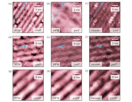
Fig. 3. (a) STM topographic images (the misorientation angle is ~3?) obtained by a qPlus sensor in a constant current mode, while AFM signals are grounded. The junction setup is Vbias=100 mV,Iset=100 pA.(b)AFM topographic images of the same FOV to(a)obtained by a qPlus sensor in a constant frequency shift mode with ?f =?6.5 Hz and Vbias=10 mV.The oscillation frequency of the quartz tuning fork is about 22.6 kHz,which is far larger than the cut-off frequency of the STM preamplifier(~1.1 kHz). A small bias voltage of 10 mV is applied to the sample,so the averaged current signal can be obtained simultaneously. The modulations of the moir′e pattern can hardly not be resolved. (c)Current image obtained from the tip simultaneously with(b).The modulations of the moir′e pattern can be resolved. The blue arrows in(a)–(c)indicate the direction of the stripe-like moir′e superlattice modulations in(a). (d)STM topographic images when the misorientation angle is ~7?. The junction setup is Vbias=100 mV,Iset=10 pA.(e)AFM topographic images of the same FOV to (d) with ?f =?7 Hz and Vbias =10 mV. The oscillation frequency of the quartz tuning fork is about 32.2 kHz. The modulations of the moir′e pattern can hardly be resolved. (f) Current image obtained from the tip simultaneously with (e). The modulations of the moir′e pattern can be resolved. The blue arrows in(d)–(f)indicate the direction of the stripe-like moir′e superlattice modulations in(d). (g)STM topographic images when the misorientation angle is ~12?. The junction setup is Vbias=10 mV,Iset=100 pA.(h)AFM topographic images of the same FOV to(g)with ?f =?8.8 Hz and Vbias =10 mV.The oscillation frequency of the quartz tuning fork is about 32.2 kHz. The modulations of the moir′e pattern can be well resolved. (i)Current image obtained from the tip simultaneously with(h). The modulations of the moir′e pattern can also be resolved.
Figure 4(a) plots the measured corrugation of the moir′e superlattice modulations in the AFM topographic image with respect to?. When the misorientation angle?is relatively small(≤3?),the moir′e pattern can not be resolved in the AFM topographic image and the corrugation is 0 pm.When the misorientation angle?increases and is larger than 10?, a sharp enhancement of the moir′e pattern corrugation above 20 pm can be found. Figure 4(b)plots the measured periodicities of the strongest moir′e pattern wave vectors from the FFT of the STM topographic images. When the misorientation angle?is relatively small (≤3?), the periodicities of the three pairs of the moir′e pattern wave vectors are similarly short. When the misorientation angle?increases and is larger than 10?, only one pair of the moir′e pattern wave vectors has the strongest intensity and a sharp increase of its periodicity is found. A similar relationship between structural relaxation and misorientation angle?has been reported in layered material MoS2.[30]The increased periodicities of the moir′e superlattice modulations increase the distance between neighboring Te–Se atom stacking, allowing lattice relaxation even though it is driven by weak VdW interaction.[30]
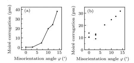
Fig. 4. (a) The measured corrugation of the moir′e pattern in the AFM topographic image with respect to ?. (b) The measured periodicities of the moir′e superlattice modulations in the FFT of the STM topographic image with respect to ?.
4. Conclusions
In summary, we successfully grow and investigate 1UC FeTe film on NbSe2single crystal with a homemade MBE–STM/AFM combined system. We find different stripe-like superlattice modulations in the STM topographic images of the grown FeTe film associated with its different misorientation angles with respect to NbSe2substrate. Comparing the experimental results with simulation by superimposing FeTe and NbSe2, we unambiguously show that the stripe-like superlattice modulations are moir′e superlattice modulations in different misorientation angles. Therefore, our results support the interface between FeTe film and NbSe2substrate is atomically sharp.
Furthermore, we find that the moir′e superlattice modulations have an electronic origin with STM–AFM combined experiments in most cases when the misorientation angle?is relatively small (≤3?). In the FM AFM topographic image,the moir′e superlattice modulations are hardly distinguished,but still clearly resolved in the simultaneously obtained current image. Since STM topographic image is more sensitive to electronic structure than AFM topographic image,we suggest that the moir′e patterns are modulations of the local density of states other than structural relaxation. However, in rare cases when the misorientation angle?is relatively large (≥10?),structural relaxation emerges and can be resolved in the AFM topographic image. Therefore, the interface system between FeTe film and NbSe2substrate may be a platform to study the influence of misorientation on the structural relaxation and/or electronic reconstruction of FeTe/NbSe2.

- Chinese Physics B的其它文章
- Modeling the dynamics of firms’technological impact?
- Sensitivity to external optical feedback of circular-side hexagonal resonator microcavity laser?
- Controlling chaos and supressing chimeras in a fractional-order discrete phase-locked loop using impulse control?
- Proton loss of inner radiation belt during geomagnetic storm of 2018 based on CSES satellite observation?
- Embedding any desired number of coexisting attractors in memristive system?
- Thermal and mechanical properties and micro-mechanism of SiO2/epoxy nanodielectrics?