Suppression of persistent photoconductivity in high gain Ga2O3 Schottky photodetectors?
2021-12-22 06:49:28HaitaoZhou周海濤LujiaCong叢璐佳JiangangMa馬劍鋼BingshengLi李炳生HaiyangXu徐海洋andYichunLiu劉益春
Chinese Physics B 2021年12期
Haitao Zhou(周海濤), Lujia Cong(叢璐佳), Jiangang Ma(馬劍鋼),Bingsheng Li(李炳生), Haiyang Xu(徐海洋), and Yichun Liu(劉益春)
Key Laboratory for UV-Emitting Materials and Technology of Ministry of Education,Northeast Normal University,Changchun 130024,China
Keywords: Ga2O3 Schottky photodetector,persistent photoconductivity,high gain,pulse voltage,oxygen vacancy
1. Introduction
Recently, Ga2O3and related materials have attracted widespread attention due to their potential applications in optoelectronic and microelectronic devices.[1–9]Although significant progress has been made in the research of Ga2O3based devices, the manipulation and understanding of its defects and related physical characteristics still demand further research,[10–18]for example, the defect-related photoconductivity gain and persistent photoconductivity (PPC) observed in Ga2O3photodetectors.[19–25]The photoconductive gain increases the responsivity of the device, which is conducive to the detection of weak light,while PPC increases the response recovery time of the device, which is not conducive to the detection of high-frequency switching light. In photodetectors based on ZnO,SnO2,InGaZnO,and GaN,the application of “interference” (for example, bending, illumination, heating and electric field) to suppress PPC in the photodetector has been proven to be efficient and feasible without affecting the high responsivity(gain).[26–31]Recently,heating and electric fields have been used in Ga2O3photodetectors to maintain high gain and effectively suppress PPC. In our previous work,[21]we studied the effect of“short-time heating”process on PPC in Ga2O3photoconductor,through which the PPC can be effectively suppressed within a few seconds. From an application point of view, the electric field may be more capable of suppressing PPC in microseconds. Hanet al.[22]and Ahnet al.[24]adopted the method proposed by Jeonet al.[26]to suppress PPC in Ga2O3three-terminal transistor by applying a pulse voltage at gate. Qiaoet al.[31]suppressed PPC in Si/Al2O3/Ga2O3heterojunction photodetectors by applying a pulse voltage. However,there is no report on the effect of the pulse voltage on PPC in a simple two-terminal Ga2O3Schottky photodetector.
In this paper, the metal–semiconductor–metal (MSM)Schottky Ga2O3photodetectors we prepared show high gain and PPC. We study the influence of pulse voltage size and width on PPC in MSM Schottky Ga2O3photodetectors.Combining the photoresponse characteristics of the prepared Ga2O3photoconductors and the unidirectional Schottky devices and the effect of pulse voltage on the PPC, a physical model related to ionized oxygen vacancies in the reversebiased Schottky junction is proposed.
2. Experimental methods
Ga2O3films were grown onc-plane sapphire substrates at room temperature by pulsed laser deposition (PLD). The substrates were sequentially cleaned with acetone,ethanol and deionized water in an ultrasonic bath for 10 min,respectively.After being cleaned,the substrates were blown dry using nitrogen gas. The distance between the substrate and the target is 4.5 cm. The background pressure and oxygen pressure in the growth chamber were fixed at 1×10?6Pa and 3×10?3Pa,respectively. The Kr excimer laser pulse energy and repetition rate were 240 mJ and 10 Hz. The as-grown Ga2O3films were subsequent thermally annealed at 600?C in oxygen ambient. The crystal structures were characterized by a Rigaku D/max-2500 x-ray diffractometer. The optical characteristics were measured by a Hitachi UH4150 spectrometer. The morphologies were characterized by scanning electron microscopy(SEM,Hitachi S-4800). Al and Au electrodes were deposited on the annealed Ga2O3films using shadow masks by vacuum thermal evaporation. The width, length and distance of the interdigital fingers in Au/Ga2O3/Au and Al/Ga2O3/Al devices are 50μm,1000μm and 20μm,respectively. The distance between the Au and Al square electrodes is 500μm for the Au/Ga2O3/Al devices. TheI–Vcharacteristics and timedependent photoresponse of the devices were measured using a Keithley 2461 sourcemeter and a system composed of a Xe lamp,a monochromator and an optical chopper.
3. Results and discussion
The XRD pattern of the Ga2O3film is shown in Fig.1(a).There are three diffraction peaks at 19.2?, 38.3?, and 59.3?,corresponding to the (-201), (-402) and (-603) crystal planes ofβ-Ga2O3, respectively.[32,33]However, the intensity ratio of(-201)and(-402)diffraction peaks is 0.031,which is lower than the theoretical value (2.2) reported in the literature.[34]This phenomenon may be caused by the overlap of the(0006)diffraction peak ofα-Ga2O3and the (-402) diffraction peak ofβ-Ga2O3.[34]Therefore, our Ga2O3film may be a mixedphase material withα(rhombohedral) andβ(monoclinic)phases coexisting, and similar results have been reported by other research groups.[35,36]The thickness of the Ga2O3film is about 290 nm,as shown in the cross-sectional image in the inset of Fig.1(a).
Figure 1(b) shows the optical transmission spectrum of the Ga2O3film. The spectrum shows a high transmittance of over 90% in the 300–800 nm, and has a cutoff at approximately 268 nm. The fitting result of the optical band-gap of the film is about 4.6 eV, as shown in the inset of Fig. 1(b).The optical band gap obtained here is consistent with the results(4–4.7 eV)reported in the literature by the PLD method at a relatively low preparation temperature (<650?C).[37,38]However, it is slightly smaller than the previously reported 4.8–5.1 eV.[39–41]This difference may be related to different tail states,crystallinity and other factors.
Figure 2(a) shows theI–Vcurve of the interdigitated Au/Ga2O3/Au device in the dark and under 254 nm illumination,in which the rectification characteristic indicates a typical Schottky contact between Au and Ga2O3. Figure 2(b) shows the responsivity and gain spectral of the device at 20 V bias.Responsivity(Rλ)and gain(Gλ)could be calculated by[21,42]
whereIλis the light current,Idis the dark current,Pλis the intensity of the illumination,Sis the effective area,his the Planck’s constant,cis the speed of light,ηis the quantum efficiency(assuming the quantum efficiency is 100%),qis the elementary charge,andλis the wavelength of illumination.The responsivity spectrum shows predominant peak (>2.5 A/W)at 230–250 nm,and the corresponding gain is>13. The UVto-visible rejection ratio that is defined as the responsivity ratio at 240 nm and that at 400 nm of around 114 is achieved in the photodetector.
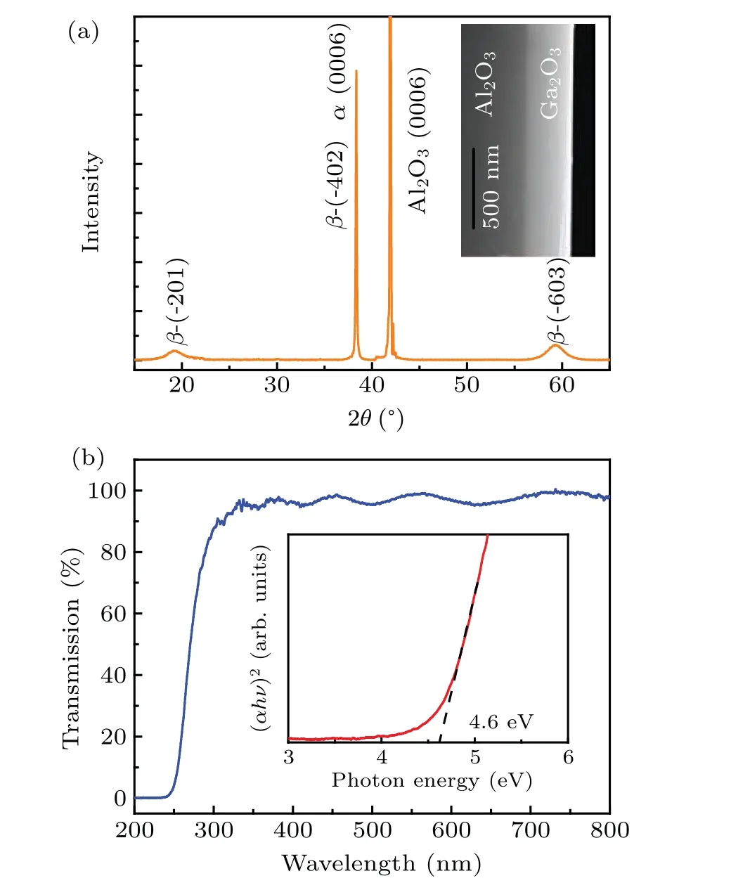
Fig. 1. (a) XRD pattern of the Ga2O3 film, the typical cross-sectional SEM image of the film(inset). (b)Optical transmittance spectra of the Ga2O3 film. The inset shows the band-gap fit.

Fig.2. (a)The I–V characteristics of the Au/Ga2O3/Au device in dark and under 254 nm illumination(446μW/cm2). The inset shows the device structure.(b)Responsivity and gain spectrum at 20 V bias in semilog scale. The inset shows the linear responsivity spectrum. (c)Time-dependent photoresponses of the device to 254 nm illumination. This includes the effect of different voltage pulses on PPC.(d)PPC current vs. the pulse voltage. (e)The time-dependent cyclic photoresponse of the device. (f)PPC current vs. the pulse width. The PPC current was measured 4 s later than the pulse voltage.
Figure 2(c) shows the time-dependent photoresponse of the Au/Ga2O3/Au device to 254 nm illumination at?20 V bias. The dark current is about 1 nA and the current increases rapidly to about 4 μA once the light illuminates on the device. After removing the light, it takes more than 5 hours for the PPC current to return to the initial dark current (black line) due to the PPC effect. In order to restrain the PPC,?15 V, +10 V, +15 V, +20 V, +25 V, and+30 V pulses with duration of 500 ms were applied to the Au/Ga2O3/Au device. As shown in Fig. 2(c), the?15 V pulse has almost no effect on the PPC current attenuation,and when +10 V, +15 V, +20 V, +25 V, and +30 V pulses are applied, the PPC current drops significantly. For comparison purpose, the PPC currents measured 4 s after the end of the pulse were used to evaluate the effect of the pulse voltage on PPC suppression. Figure 2(d) shows the variation of the PPC current with the pulse voltage. The greater the applied positive pulse voltage, the more the PPC current drops. The PPC current corresponding to pulse voltages of+20 V,+25 V and+30 V drops sharply from 320 nA without pulse voltage to 14–11 nA. Taken the +20 V pulse as an example, timedependent photoresponse cycling showed that the pulse voltage not only suppressed PPC,but also was harmless to the stability and repeatability of photoresponse(Fig.2(e)). When the+20 V pulse duration increases from 100 ms to 4000 ms,the corresponding PPC current decreases from 16.2 nA to 13.3 nA(Fig.2(f)). Obviously,applying a pulse voltage can make the response recovery time of the device reach 100 ms. Note that,as shown in Fig. 2(c), after the pulse voltage is removed, the current has a short process of rapid rise.This may be related to the rapid extraction/injection process of electrons in the Schottky junction region when the bias at both ends of the Schottky junction changes instantaneously.
Figure 3(a)shows theI–Vcharacteristics of the interdigitated Al/Ga2O3/Al device in the dark and under 254 nm illumination,in which a linearI–Vcurve indicated that Al and Ga2O3film formed a typical Ohmic contact. The responsivity is 7.9 A/W at 254 nm, and the corresponding gain is 41.Figure 3(b) shows the time-dependent photoresponses of the Al/Ga2O3/Al device to 254 nm illumination at?20 V bias,in which one can also see an obvious PPC effect. But unlike the Au/Ga2O3/Au device,the pulse voltages of?15 V,+20 V and +30 V (pulse duration was also 500 ms) have almost no contribution to PPC current attenuation(Fig.3(b)).

Fig. 3. (a) The I–V characteristics of the Al/Ga2O3/Al device in dark and under 254 nm illumination (44 6 μW/cm2). The inset shows the device structure. (b)Time-dependent photoresponses of the device to 254 nm illumination.
In our previous report, the gain and PPC in the Ga2O3

It is known that Au/Ga2O3/Au device is composed of two Schottky junctions, in which one Schottky junction is always reverse-biased and the other is forward-biased. In order to verify whether the forward-biased Schottky junction or the reverse-biased Schottky junction made more contribution to PPC suppression,we fabricated an Al/Ga2O3/Au device with Al and Au square electrodes. Because the Schottky contact is at the Au electrode and the Ohmic contact is at the Al electrode,theI–Vcurve of the Al/Ga2O3/Au device in dark shows significant rectification characteristics (Fig. 4(a)). As shown in Fig.4(b),when the Ga2O3/Au Schottky junction is forwardbiased with a bias of +20 V, a?20 V pulse with duration of 500 ms is applied to the device,and the PPC current is almost unaffected. On the contrast, when the Ga2O3/Au Schottky junction is reverse-biased with the bias of?20 V,the PPC current is reduced dramatically once a+20 V pulse with 500 ms duration is applied to the device,as shown in Fig.4(c). Therefore, the pulse voltage will take effect upon suppressing PPC only in reverse biased Ga2O3/Au Schottky junction.
As we all know,the characteristics of Schottky photodetector are mainly related to the Schottky barrier, especially when the junction is under a reverse bias. In the metal/Ga2O3Schottky junction, the metal/Ga2O3interface trap and the hole self-trapped trap near the Schottky junction can trapping photo-generated holes, which are considered to be two main mechanisms that may reduce the height of the Schottky barrier.[46–48]If the interface trap state trapping holes is the main mechanism of PPC in our Schottky device. Then,only under the forward bias,it is almost possible to make the electrons tend to the interface to recombine the trapped holes and achieve the effect of suppressing PPC. However, our experiments show that applying +10 V and +15 V pulses can suppress PPC, and the bias on the Schottky junction at this time is?10 V and?5 V under reverse bias (Fig. 2(c)). The self-trapped hole model near the Schottky junction believes that the electron–phonon coupling of the lattice is so strong that the holes in the valence band induce local distortion of the ion positions in the lattice,thereby generating an electrostatic potential that locates the holes.[48]Since the self-trapping of holes is an inherent material property,this model will produce gains in any combination of Schottky metal and Ga2O3surface orientations.[48]However, in our previous work, as the annealing temperature of the Ga2O3film increased to 800?C,the corresponding MSM Schottky device’s responsivity(gain)at 254 nm decreased from 136 A/W (706) to 3×10?4A/W(0.0016).[23]Obviously,these devices do not all show significant gains,that is,the gains are not all greater than 1.

Fig. 4. (a) The I–V characteristics of Au/Ga2O3/Al device with square electrodes in dark. The inset shows the device structure. Panels (b)and(c)show the time-dependent photoresponses of the device to 254 nm illumination under forward bias and reverse bias,respectively. The?20 V and+20 V pulses were selected for demonstration,respectively.
In fact,our previous work and literature results show that as the oxygen vacancy concentration in Ga2O3decreases,the responsivity (gain) and PPC of the Schottky device decrease and weaken, respectively.[4,23,25,49]Therefore, the gain and PPC of our Ga2O3Schottky photodetectors are more likely to be related to the oxygen vacancy in Ga2O3.


Fig. 5. Schematic diagram of the energy band at Au/Ga2O3 Schottky junction: (a) initial in dark; (b) under illumination; (c) after illumination has removed;(d)applying a+20 V pulse voltage;(e)after the pulse voltage ends.
Table 1 shows some important parameters of Ga2O3photodetectors that have been reported.With the responsivity provided in the literature, the gain can be calculated. Our MSM devices have high responsivity and gain. More importantly,the pulse voltage suppression PPC makes the response recovery time of the device 0.1 s, so it achieves a fast response recovery speed while maintaining high responsivity(gain).
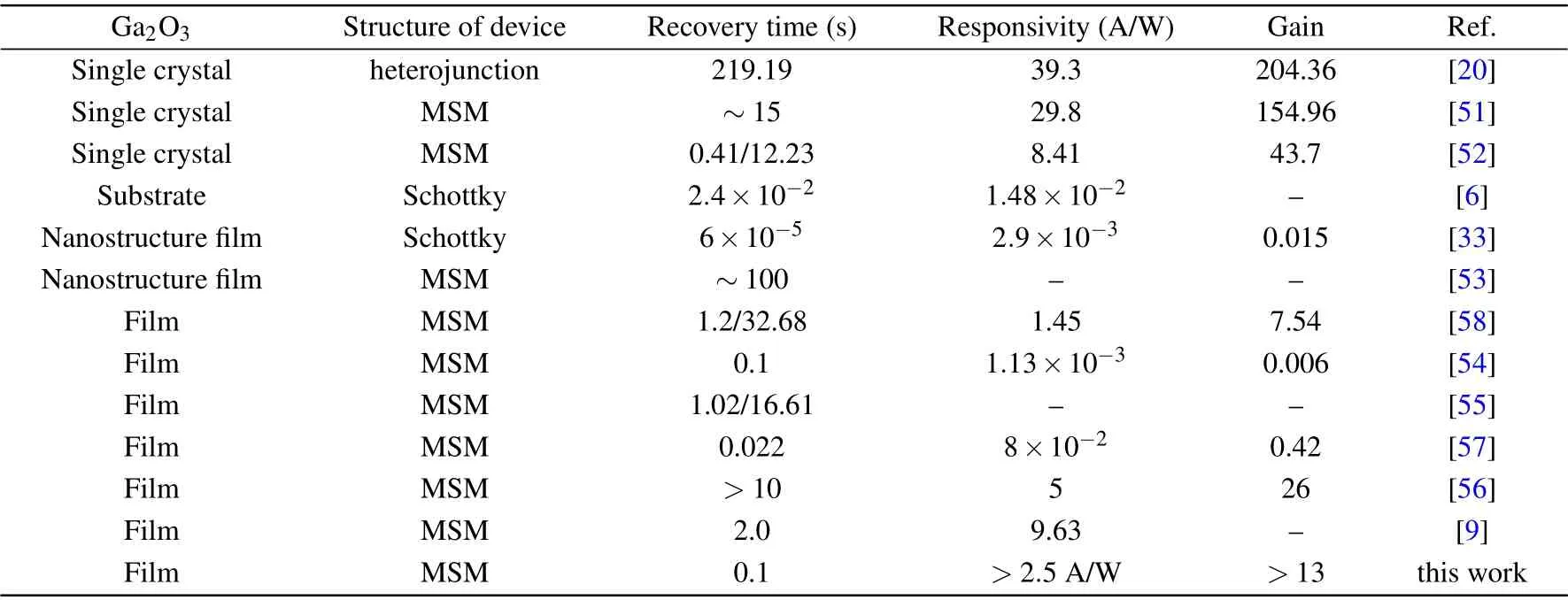
Table 1. Comparison of the photoresponse parameters between the Ga2O3 based photodetectors.
4. Conclusions

- Chinese Physics B的其它文章
- Modeling the dynamics of firms’technological impact?
- Sensitivity to external optical feedback of circular-side hexagonal resonator microcavity laser?
- Controlling chaos and supressing chimeras in a fractional-order discrete phase-locked loop using impulse control?
- Proton loss of inner radiation belt during geomagnetic storm of 2018 based on CSES satellite observation?
- Embedding any desired number of coexisting attractors in memristive system?
- Thermal and mechanical properties and micro-mechanism of SiO2/epoxy nanodielectrics?