Effects of Electron Irradiation at Different Energy and Fluences on Electrical Properties of InP HEMT Structure
2021-12-15 13:47:18ZHOUShuxingFANGRenfengCHENChuanliangZHANGXinWEIYanfengCAOWenyuLEIShulaiAILikun
原子能科學技術 2021年12期
ZHOU Shuxing, FANG Renfeng, CHEN Chuanliang, ZHANG Xin, WEI Yanfeng, CAO Wenyu, LEI Shulai, AI Likun
(1.Hubei Key Laboratory of Low Dimensional Optoelectronic Materials and Devices, Hubei University of Arts and Science, Xiangyang 441053, China; 2.State Key Laboratory of Functional Materials for Informatics, Shanghai Institute of Microsystem and Information Technology, Chinese Academy of Sciences, Shanghai 200050, China)
Abstract: The InGaAs/InAlAs InP high electron mobility transistor (HEMT) structures with lattice-matched channels were grown by gas source molecular beam epitaxy (GSMBE). Effects of electron irradiation at different energy and fluence on the electrical properties of InP HEMT structures were comprehensively investigated. It was found that high energy electron beam has an obvious effect on the electrical properties of two-dimensional electron gas (2DEG) at the same fluence of 2×1015 cm-2. After the fluence exceeding 4×1014 cm-2, the 2DEG mobility and density begin to decrease obviously, and did not reach saturation until the fluence was more than 3×1015 cm-2. These changes could be mainly attributed to the aggregation of irradiation-induced defects at the channel heterogeneous interface with the increase of displacement damage dose.
Key words:InP HEMT; two-dimensional electron gas; electron irradiation; displacement damage
1 Introduction
With the development of space exploration to deep space, high-speed data transmission and high-precision detection are very important. Low noise amplifier with high frequency, high sensitivity and low noise figure is urgently needed to be applied in deep space communication system[1-3]. Attributed to the great electrical transport properties of the two-dimensional electron gas (2DEG) for InAlAs/InGaAs hetero-junction structure, InP high electron mobility transistor (InP HEMT) has achieved tremendously superior performance, such as low noise figure, high frequency, low power consumption and excellent power gain and so on[4-5]. Benefiting from molecular beam epitaxy (MBE) and electron beam lithography (EBL) technologies, the current generation of InP HEMT has increased the current gain cut-off frequency (fT) and maximum oscillation frequency (fmax) to approximately 0.61 THz and 1.5 THz, respectively[6]. At present, InP HEMT integrated circuits used for all receiver and transmitter functions, including power amplification and low noise amplification directly at 850 GHz, as well as frequency conversion have been reported[3]. Therefore, InP HEMT integrated circuits have excellent potential for terahertz-wave transceiver communication system in deep-space exploration, satellite remote sensing and aerospace.
However, spacecraft in space are faced with severe radiation environment including earth radiation belt, solar flare and galactic cosmic ray. InP HEMT integrated circuits applied in the transceiver communication system will inevitably be affected by various rays and high-energy particles, such as protons, electrons, heavy ions and other secondary atomic radioactive particles[7-9]. Among them, high-energy particle such as electron, which is one of the main particles in harsh space environment, will introduce lattice defects and atomic mixing in the heterogeneous interface due to energy loss[10]. This will lead to the degradation of key parameters of HEMT devices such as 2DEG density and mobility, minimum noise figure (fmin), cut-off frequency, maximum oscillation frequency, and even device failure in space communication system, which seriously affects the stability and accuracy of space communication, and threatens the safe and reliable operation of spacecraft[11-13]. Admittedly, the irradiation damage effects of various HEMT devices such as GaN HEMT, GaAs HEMT, InP HEMT, InAs/AlSb HEMT have been widely reported[14-17]. Nonetheless, majority work on InP HEMT devices was focused mainly on the performance of the direct current (DC) and radio frequency (RF)[17-19]. Much less attention was given to the irradiation effects on the electrical properties of InP HEMT structures. Actually, the electron mobility (μ) and density (Ns) of two-dimensional electron gas (2DEG) are two important parameters that affect the frequency, power gain and noise figure of HEMT devices. Therefore, it is very important to study the influence of electron irradiation on the two-dimensional electron gas (2DEG) for analyzing the radiation degradation mechanism of HEMT devices.
In this paper, electron irradiation at different energy from 1.0 MeV to 1.8 MeV was carried out on the lattice-matched InP HEMT structures with various fluence ranging from 1×1014cm-2to 1×1016cm-2. The changes and radiation damage mechanism of 2DEG density and electron mobility were carefully investigated before and after electron irradiation. This research can provide an effective analytical basis for further study on the radiation degradation mechanism of InP HEMT devices.
2 Experiment
The lattice-matched InP InGaAs/InAlAs HEMT epitaxial structure was grown on semi-insulating (100) InP substrates by a V90 gas source molecular beam epitaxy (GSMBE) system. Detailed growth details can be found in the references [20-22]. The basic HEMT epitaxial structure is shown in Table 1. The structure is comprised of an InP substrate, a 500-nm-thick InAlAs buffer layer, a 15-nm-thick InGaAs channel layer, a 3-nm-thick InAlAs spacer layer, a Siδ-doped sheet layer, a 8-nm-thick InAlAs barrier layer, a 4-nm-thick InP etching stopper layer, a 15-nm-thick n+-InAlAs cap layer, a 15-nm-thick n+-InGaAs cap layer and a 10-nm-thick n+-In0.65Ga0.35As cap layer.
All the epitaxial samples taken from the same wafer of the InP HEMT structure were vertically irradiated at room temperature with different electron energy from 1.0 MeV to 1.8 MeV and fluence up to 1× 1016cm-2. The electron beam can go straight through the InP HEMT structure and make displacement damage not only in the QW active layer but also in the buffer and substrate layers as well[23]. Accordingly, the two-dimensional electron gas (2DEG) density and electron mobility are measured by Accent HL5500 Hall system at room temperature and 77 K as a function of the electron energy and irradiation fluence, respectively. The hall data of the as-grown InGaAs/InAlAs HEMT structure is shown in Table 2.
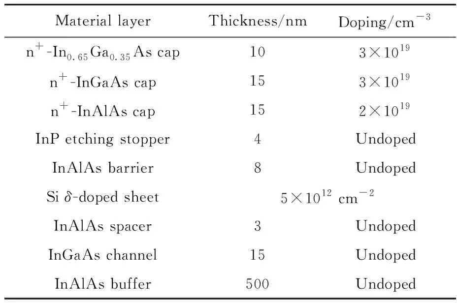
Table 1 Epitaxial structure of lattice-matched InP HEMT
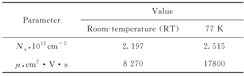
Table 2 Hall data of as-grown InGaAs/InAlAs HEMT structures
3 Results
3.1 Effects of electron energy
Generally, the 2DEG properties of the HEMT epitaxial structure are strongly affected by particle irradiation energy[24-25]. In order to study the effect of the electron energy on the 2DEG properties of InGaAs/InAlAs InP HEMT epitaxial structure, a series of the lattice-matched InP HEMT structures were irradiated at different electron irradiation energy ranging from 1.0 MeV to 1.8 MeV at the fluence of 2×1015cm-2.Fig.1 shows the dependence of electron mobility and 2DEG density with electron energy measured at RT and 77 K, respectively.Fig.1a shows that the electron mobility descends rapidly with the increase of electron energy at room temperature and 77 K, respectively, while the degradation of electron mobility at 77 K is more serious than that at room temperature for samples irradiated with the same electron energy at the fluence of 2×1015cm-2. As shown in Fig.1b, the 2DEG density decreases slowly with the increase of electron irradiation energy at room temperature and 77 K, respectively, while the 2DEG density at 77 K also decreases more seriously than that at room temperature.
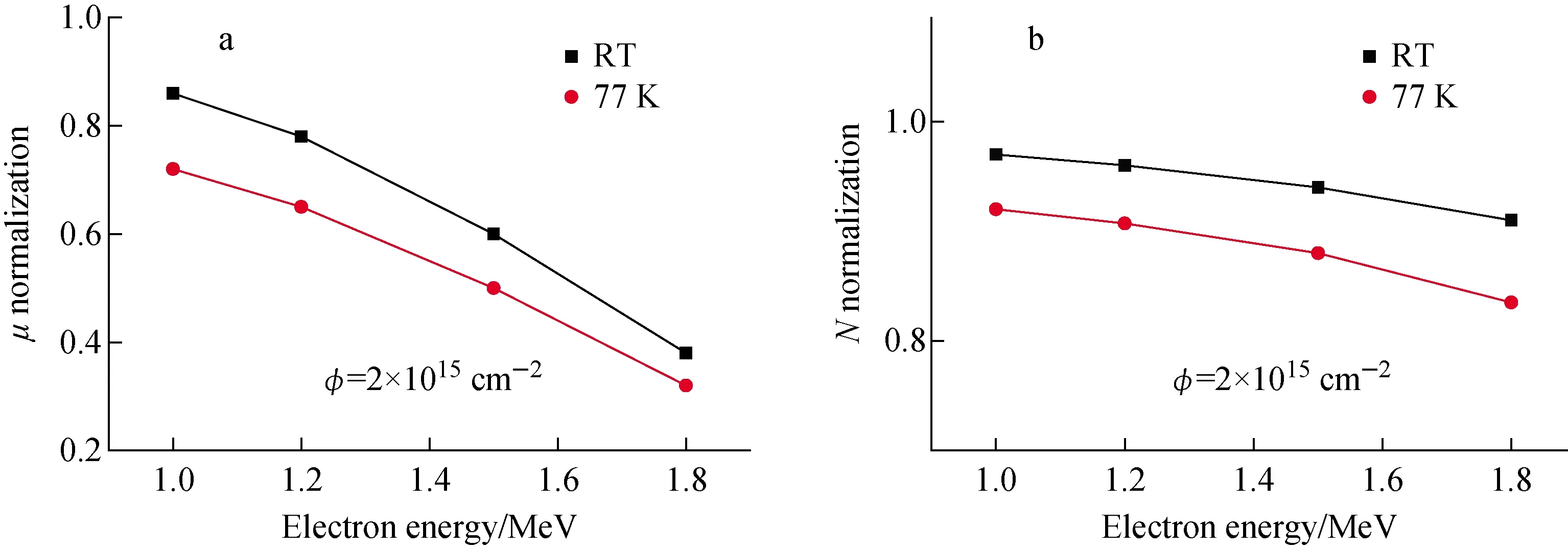
Fig.1 Dependence of Hall mobility (a) and 2DEG density (b) on electron irradiation energy measured at RT and 77 K
3.2 Effects of electron irradiation fluence
Normally, the 2DEG properties of the HEMT epitaxial structure are strongly affected by particle irradiation fluence[26-27]. In order to study the effect of the electron irradiation fluence on the 2DEG properties, a series of the lattice-matched InP HEMT structure were irradiated at the electron energy of 1.5 MeV with various fluence ranging from 1×1014cm-2to 1×1016cm-2. The electron mobility and density of two-dimensional electron gas (2DEG) before and after irradiation are shown in Fig.2. When the irradiation fluence is lower than 4×1014cm-2, there is no obvious effect on the electrical transport properties of the InP HEMT structure. As shown in Fig.2a, the decrease of electron mobility is less than 5%, while the degradation of 2DEG density is less than 1.5% in Fig.2b. With the irradiation fluence exceeding 4×1014cm-2, the electron mobility begins to decrease obviously in Fig.2a, while the 2DEG density also continues to decline rapidly, as is shown in Fig.2b. Both of them showed a rapid downward trend between the irradiation fluence of 4×1014cm-2-3×1015cm-2. Until the irradiation fluence exceeds 3×1015cm-2, the electron mobility and 2DEG density decrease slowly and finally reach saturation, as is shown in Fig.2. However, the degradation of electron mobility and 2DEG density at 77 K is more serious than that at room temperature for samples irradiated at 1.5 MeV electron energy under the fluence of 4×1014cm-2-1×1016cm-2.
4 Discussions
The 2DEG transport characteristics of InP HEMT structure are mainly affected by the energy band structure of InGaAs/InAlAs heterostructure and various scattering processes.

Fig.2 Dependence of Hall mobility (a) and 2DEG density (b) on irradiation fluence measured at RT and 77 K
The total mobility (μt) of two-dimensional electron gas(2DEG) is mainly determined by these scattering mechanisms (μn), such as ionized impurity scattering (including remote impurity scattering and background impurity scattering), lattice vibration scattering, interface scattering and alloy disorder scatterings[21]. After electron irradiation, the 2DEG transport characteristics of InP HEMT structure materials will be degraded by electron irradiation damage. Electron irradiation damage results from the interaction between electrons and lattice atoms of InP HEMT structure, which can be divided into ionization effect and displacement effect. For the InP HEMT structure materials, electron irradiation mainly causes displacement damage effects. The displacement damage effects creates defect energy levels in the quantum well region of structural materials that can act as trapping and recombination centers and cause changes in important parameters, such as 2DEG density and electron mobility. With the electron irradiation fluence exceeding a certain threshold, the 2DEG density and electron mobility will be affected by the number of irradiation-induced damage defects in the quantum well region, as is shown in Fig.2, which stems from the displacement damage effects.
In fact, when an energetic electron with energyEis incident on InP HEMT materials, the energy transferred in displacement damage is known as non-ionizing energy loss (NIEL), which is described as[28-29]
[dσ(θ,E)/dΩ]dΩ
(1)
whereNis Avogadro’s number,Ais the atomic mass, maximum energy transfer occurs forθ=π,T(θ,E) is the transferred energy due to an incident electron scattered through an angleθin the center of mass system,L[T(θ,E)] is the Lindhard partition factor, which gives the fraction of transferred energy that is nonionizing[30], dσ(θ,E)/dΩis the differential cross-section for elastic scattering of electrons scattered into a solid angle increment dΩand the integral has a lower limit of scattering angleθminfor which the recoil energy equals the threshold for displacement[29]. It implies that the NIEL caused by electron irradiation is not only related to the properties of the irradiated materials, but also related to the incident electron energy. It can be concluded from the above formula that the electron NIEL increases with the electron energy from 0.5 MeV to 10 MeV, which has been proved by Summers[29]. Normally, the magnitude of displacement damage effects can be expressed by displacement damage dose (DDD). In what follows, the total displacement damage dose can be described as the product of NIEL(E)with the electron irradiation fluenceφ(E), which means that the incident electrons with higher energy lead to a larger displacement damage dose at the same irradiation fluence. Meanwhile, the number of radiation-induced defects are positively proportional to the displacement damage dose. With the increase of electron irradiation energy from 1.0 MeV to 1.8 MeV at the fluence of 2×1015cm-2, the number of radiation-induced defects in InP HEMT structure will increase, leading to the decrease of 2DEG density and electron mobility, as is shown in Fig.1. The similar phenomena were also found in GaAs HEMT structural irradiated by various electron energy[31].
When the electron irradiation energy is constant, the decrease of 2DEG density and electron mobility is related to the concentration of radiation-induced defects and its scattering, which is related to the electron irradiation fluence. Compared to the concentration of material growth defects, the concentration of defects induced by electron irradiation is very seldom at the irradiation fluence of below 4×1014cm-2. So the degradation of 2DEG density and electron mobility is not significant, as is shown in Fig.2. After the irradiation fluence exceeds 4×1014cm-2, a large number of radiation-induced defects gather at the heterogeneous interface of InGaAs/InAlAs channel with the increase of the irradiation fluence and capture the two-dimensional electron gas, which can greatly affects the electron mobility of 2DEG. At the same time, the radiation-induced interface trap at the heterogeneous interface of InGaAs/InAlAs channel also changes the energy shape of quantum well since the additional trapped charges appears because of the carrier captured by the radiation-induced interface trap, which weakens the built-in electric field of the heterogeneous InGaAs/InAlAs channel interface. As a result, the band curvature decreases and the triangular potential becomes shallow, resulting in the decrease of 2DEG density. This phenomenon has been reported in GaN HEMT structure irradiated by proton[8]. Compared with the total as-grown scattering factors before irradiation, including ionized impurity, lattice vibration, interface roughness, alloy disorder and so on, the scattering of radiation-induced defects on the transport properties of 2DEG become a factor that cannot be ignored after the fluence exceeding 4×1014cm-2. Since the concentration of the irradiation-induced defect is quickly increased with the increase of irradiation fluence before the fluence below 3×1015cm-2. It turns out that the scattering of radiation-induced defects increases with the irradiation fluence. Consequently, the 2DEG density and electron mobility degrades quickly between the fluence ranging from 4×1014cm-2to 3×1015cm-2, as is shown in Fig.2. This similar experimental phenomenon has also been observed in GaAs HEMT structural irradiated by electron between the fluence ranging from 2.5×1014cm-2to 1×1015cm-2[31].
After the irradiation fluence exceeding 3×1015cm-2, the concentration of irradiation-induced defects increases slowly with the irradiation fluence, so does the scattering of radiation-induced defects. It is because that the generation and recombination of radiation-induced defects will reach a dynamic equilibrium at high irradiation fluence. Even though the irradiation fluence is increased, the concentration of radiation-induced defects will not increase too much, and the decrease of 2DEG density and electron mobility will slow down until reach saturation, as is shown in Fig.2. This experimental phenomenon also exists in GaAs HEMT structure irradiated by electron with high fluence[31].
5 Conclusion
In summary, we have investigated the effect of electron irradiation at different energy and fluence on the electrical properties of InP HEMT structures. After electron irradiation, the aggregation of irradiation-induced defects at the channel heterogeneous interface, which result from the increase of displacement damage dose, will degrade the 2DEG density and electron mobility. It was found that high energy electron beam has an obvious effect on the electrical properties of 2DEG at the same fluence of 2×1015cm-2. Between the fluence of 4×10¹⁴-3×1015cm-2, the 2DEG density and electron mobility degrade evidently, and did not reach saturation until the fluence exceeding 3×1015cm-2.