Sphere-shaped SiGe micro/nanostructures with tunable Ge composition and size formed by laser irradiation?
2021-09-28 02:18:12XinxinLi李欣欣ZhenDeng鄧震SenWang王森JinbiaoLiu劉金彪JunLi李俊YangJiang江洋ZiguangMa馬紫光ChunhuaDu杜春花HaiqiangJia賈海強WenxinWang王文新andHongChen陳弘
Chinese Physics B 2021年9期
Xinxin Li(李欣欣),Zhen Deng(鄧震),Sen Wang(王森),Jinbiao Liu(劉金彪),Jun Li(李俊),Yang Jiang(江洋),Ziguang Ma(馬紫光),Chunhua Du(杜春花),4,Haiqiang Jia(賈海強),7,Wenxin Wang(王文新),7,and Hong Chen(陳弘),7,?
1Key Laboratory for Renewable Energy,Beijing Key Laboratory for New Energy Materials and Devices,Beijing National Laboratory for Condensed Matter Physics,Institute of Physics,Chinese Academy of Sciences,Beijing 100190,China
2University of Chinese Academy of Sciences,Beijing 100049,China
3Center of Materials and Optoelectronics Engineering,University of Chinese Academy of Sciences,Beijing 100049,China
4The Yangtze River Delta Physics Research Center,Liyang 213000,China
5Key Laboratory of Microelectronics Devices and Integrated Technology,Institute of Microelectronics,Chinese Academy of Sciences,China
6Beijing National Laboratory for Condensed Matter Physics,Institute of Physics,Chinese Academy of Sciences,Beijing 100190,China
7Songshan Lake Materials Laboratory,Dongguan 523808,China
Keywords:SiGe,micro/nanospheres,laser irradiation
1.Introduction
SiGe micro/nanostructures have attracted much interest from both academia and industry due to their intriguing electrical and optical properties suitable for novel electronic and optoelectronic chips that are compatible with the standard complementary metal–oxide–semiconductor technology.[1–4]Up to now,two methods have been used to fabricate such micro/nanostructures.(i)Growth on one substrate via the Stranski–Krastanow mode,called the bottom-up method.With this method it is complicated to control the shape and composition of the SiGe micro/nanostructures.[5–8](ii)Fabrication by a top-down approach,such as wet etching,[9]reactive ion etching,[10–12]ion beam etching[13]or metal-assisted chemical etching.[14]
Of the above methods,laser irradiation is an easy to operate technology that has a rapid and localized energy process together with a wide range of tenability.[15,16]It can thus induce various reactions in a highly selective and localized manner,and allow precise control of annealing in the desired region.This technology has been used to fabricate micro/nanostructures on substrate surfaces in several material systems[17–19]such as II–VI,[20]III–V[21]and IV compound semiconductors.[22]Laser irradiation has been used with SiGe materials to prepare micro/nanostructures with different aspect ratios and shapes,and these have been studied in depth.[13,18,23,24]However,most such structures are islands or other structures,and there are few reports on spherical structures formed by laser irradiation.
Our previous work proposed a convenient way to fabricate a virtual SiGe template with Ge filling the porous Si(PSi)prepared by electrochemical(EC)etching,where the thickness and Ge composition of the template can be easily controlled.[25]In this paper,we show that SiGe spheres can be fabricated by laser irradiation.In this approach,the diameter can be controlled by the energy density of laser excitation.By characterizing the microstructure and composition,we are able to confirm that the major component of the microspheres is SiGe alloy,and the Ge composition is almost uniform in the SiGe microspheres.The as-prepared SiGe micro/nanospheres have great potential for use in SiGe-based micro/optoelectronic devices.
2.Materials and experiments
Figure 1 illustrates the process flow of the preparation for SiGe micro/nanospheres.First,the virtual SiGe template was prepared by Ge filling the PSi from EC etching,as described in detail in the experimental section of Ref.[25].In Ref.[25],the PSi was well filled with Ge and became the SiGe template with an abrupt interface above the bulk Si substrate after Ge deposition.The thickness of the SiGe template layer was about 2μm;the energy-dispersive x-ray spectroscopy(EDS)maps revealed a uniform distribution of Ge and Si in the template along the direction parallel to the wafer surface.Then,in order to form the SiGe microspheres,laser irradiation was performed at room temperature in a nitrogen(N2)ambient to avoid oxidation.During the irradiation process,the samples were irradiated at different energies with a 532 nm laser controlled by the laser excitation current over an area of 2×10 mm2;the irradiation time was 100 s for all samples.
The morphologies of the as-prepared samples were observed by a scanning electron microscope(SEM;Hitachi Instruments SU5000)with an operating voltage of 20 kV,coupled to EDS mapping to reveal the spatial distribution of elements.The size of the detailed morphologies and the composition of the fabricated micro/nanospheres were inferred by transmission electron microscopy(TEM;JEM-ARM200F).In order to obtain information on the quality of the micro/nanosphere crystals,micro-Raman spectroscopy analysis(JY-T64000)was carried out at room temperature using backscattering geometry with a 532 nm laser as the excitation source.
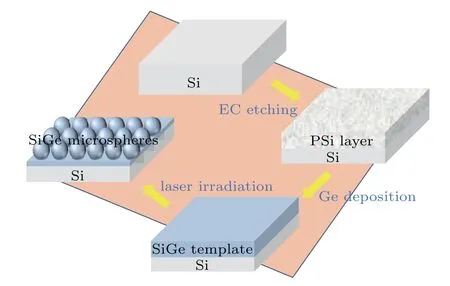
Fig.1.Schematic of the fabrication of SiGe micro/nanospheres.
3.Results and discussion
In order to form the SiGe micro/nanospheres,laser irradiation was performed in a N2ambient using an excitation wavelength of 532 nm.Two samples were exposed and annealed at a laser energy density of 0.23 J/cm2and 0.90 J/cm2,respectively;these samples are referred to as Sam-A and Sam-B,respectively.Top-view and cross-sectional SEM were performed to analyze the surface morphologies and shapes of the micro/nanostructures,as shown in Fig.2.After the laser irradiation,sphere-like nanoislands were formed on the surface.With the low energy density(0.23 J/cm2)laser irradiation,compact spheres were formed on the surface with a small diameter of about 200 nm,as shown in Figs.2(a)and 2(c).On increasing the energy density to 0.90 J/cm2,the diameter of the spheres became larger(~960 nm),the density of the spheres decreased and the thickness of SiGe template became thinner.These results suggest that the as-formed SiGe micro/nanostructures exhibit different appearances under irradiation with different laser energy densities.The probable reason could be that the energy absorbed from the laser is transformed into heat energy and then transferred internally in the SiGe template,which will reshape the template into a more stable cluster.[26]Unlike the self-assembled SiGe islands with the shape of irregular islands or cones reported in previous researches,[13,18,24]this transformation process from SiGe template to regular spheres upon laser irradiation is very similar to the formation of metal self-organized nanoballs with thermal annealing,[27]and is mainly due to the loose precursors formed by deposition of Ge into the PSi.The main process is that the nonequilibrium state clusters reshape and attempt to obtain a local minimum energy state(regular spherical particle).[28]
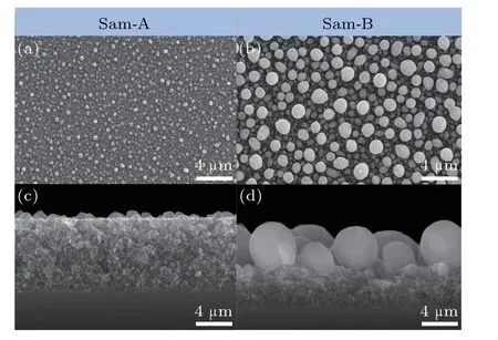
Fig.2.SEM images of the samples:(a)top view of Sam-A,(b)top view of Sam-B,(c)cross-sectional view of Sam-A,(d)cross-sectional view of Sam-B.
To obtain the crystal information on the SiGe spheres,TEM measurements of Sam-B with different magnifications and selected area electron diffraction(SAED)patterns of the SiGe micro/nanosphere were carried out.A well-defined,nearly spherical outline is observed with the low magnification in Fig.3(a)and more details can be seen with a magnification of 50000×in Fig.3(b).A microsphere with a diameter of 960 nm is clearly distinguishable from the SiGe template in Fig.3(b).Unlike the loose structure of the SiGe template,the material in the microspheres fabricated by laser irradiation is more compact and there is no visible pore network.The overall thickness also decreases from the original 2μm to about 1.165μm,which is consistent with the transition from a loose templated structure to a compact spherical structure.Unfortunately,there is a crack in the spherical structure which may be due to absorption of insufficient energy from the laser which cannot support the complete fusion of the SiGe template.On the other hand,the well-arranged electron diffraction patterns in Fig.3(c)also indicate that the prepared SiGe micro/nanosphere has a high quality,rather than the loose combination of PSi and Ge before laser irradiation.
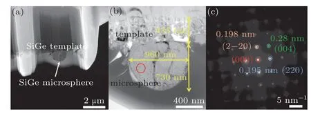
Fig.3.Cross-sectional TEM images of the SiGe micro/nanosphere in Sam-B with different magnifications:(a)10000×,(b)50000×.(c)Selected area electron diffraction patterns of the red circle in(b).
Information about the spatial distribution of elements inside the microspheres can be obtained by EDS mapping in high-angle annular dark-field(HAADF)scanning TEM(STEM)mode.The EDS maps in Figs.4(a)and 4(b)reveal high uniformity of Si and Ge in the microspheres for both horizontal and vertical directions.It should be noted that the Si and Ge signals outside the microsphere are attributed to the spattering of SiGe dust from ion cutting process in sample preparation.Furthermore,EDS line scanning counts in Fig.4(c)exhibit more details about the distribution of Si and Ge composition.The black and red dots,which represent the distribution of Si and Ge,respectively,are relatively uniform with small fluctuations inside the SiGe microsphere(blue background in Fig.4(c)).These results from TEM and EDS fully demonstrate that the as-prepared SiGe micro/nanospheres in this study have high uniformity in all spatial directions.
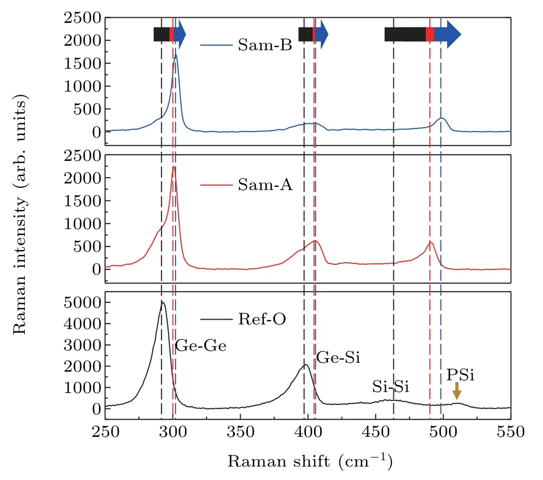
Fig.5.Room temperature micro-Raman scattering spectra of the samples before and after laser irradiation.The black,red and blue dotted lines are used to identify the peaks of the three modes in SiGe alloy,presented for Ref-O,Sam-A and Sam-B,respectively.
A sensitive technique for detecting SiGe alloy is Raman spectroscopy.[29,30]Figure 5 shows the micro-Raman spectra of Sam-A and Sam-B,as well as a sample without laser irradiation,named Ref-O,for comparison.Overall,all the spectra exhibit the typical Stokes Raman spectrum of SiGe alloys with three peaks observed around 300 cm?1,400 cm?1and 500 cm?1,corresponding to the so-called Ge–Ge,Si–Ge and Si–Si local modes,respectively.After laser irradiation,the full width at half maximum(FWHM)of the Ge–Ge peak decreases obviously and a small shoulder representing pure Ge appears on the left,while the peak of PSi even disappears in Sam-A.This phenomenon is more obvious in Sam-B with the higher laser irradiation energy,where the shoulder is further decreased so as to become almost invisible.Combined with the EDS results in Fig.4 and the electron diffraction pattern in Fig.3(c),it can be concluded that the major component of micro/nanospheres formed on the surface of the Si/Ge template with laser irradiation is SiGe alloy.At the same time,with the increase in laser energy,the peaks of the three modes all tend to move to higher Raman shifts accompanied by a decrease in the peak intensity ratios of Ge–Ge and Ge–Si modes,indicating the decreasing Ge composition in the formed spheres,consistent with the fact that the formation of larger micro/nanospheres requires more material with lower Ge composition from the deeper layer.This result indicates that the Ge composition inside the formed SiGe spheres can be effectively adjusted by controlling the laser intensity.The Ge composition of the SiGe micro/nanospheres formed in Sam-B is estimated to be about 0.43 following the method described in the literature.[30]
4.Conclusion
In summary,uniform SiGe micro/nanospheres have been successfully fabricated by laser annealing of a SiGe template.The results of SEM measurement and micro-Raman spectroscopic analyses show that the diameter and Ge composition of such structures could be tuned and controlled by manipulating the laser energy and irradiation time combined with the method for fabricating the SiGe template.By characterizing the microstructure and composition with SEM and TEM measurements,we can confirm that the SiGe micro/nanospheres are of good quality and the Ge composition inside them is almost uniform.These SiGe micro/nanospheres are expected to be useful as templates for some special Ge-related material growth and device fabrication,which could be useful for various micro/optoelectronic applications.
Acknowledgment
We appreciate the financial support from the Center for Clean Energy and Huairou Division,Institute of Physics,Chinese Academy of Sciences.
- Chinese Physics B的其它文章
- Origin of anomalous enhancement of the absorption coefficient in a PN junction?
- Protection of isolated and active regions in AlGaN/GaN HEMTs using selective laser annealing?
- First-principles study of plasmons in doped graphene nanostructures?
- Probing thermal properties of vanadium dioxide thin films by time-domain thermoreflectance without metal film?
- An improved model of damage depth of shock-melted metal in microspall under triangular wave loading?
- Signal-to-noise ratio of Raman signal measured by multichannel detectors?