A Novel De-Embedding Technique of Packaged GaN Transistors
2021-07-19 06:08:06WEIXinghuiCHENXiaofanCHENWenhuaZHOUJunmin
ZTE Communications 2021年2期
WEI Xinghui,CHEN Xiaofan,CHEN Wenhua,ZHOU Junmin
(Tsinghua University,Beijing 100084,China)
Abstract: This paper presents a novel de-embedding technique of packaged high-power transistors.With the proposed technique, the packaged model of the power amplifier (PA)tube can be divided into the frequency independent de-embedded intrinsic device (DID)and the frequency dependent internal parasitic network (IPN),which is of great help in reducing the design complexity of a broadband PA.Different from the conventional technique of parasitic extraction, the proposed technique only requires external measurements.The frequency independent characteristic of DID is verified and the IPN is modeled and calibrated for a 50 W gallium-nitride (GaN)transistor.At last, a broadband Doherty PA is fabricated with the de-embedding technique.According to the measured results,the PA exhibits satisfactory power and efficiency performance.
Keywords:de-embedding;power amplifier;intrinsic device;parasitic network
1 Introduction
With the rapid development of wireless communications, especially the emerging 5G, the power amplifier (PA)is expected to handle broad bandwidth, high power, and high efficiency simultaneously.With advantages like large power capacity, high efficiency, and high breakdown voltage, gallium-nitride(GaN)power devices make themselves ideal candidates for such applications[1].
However, the traditional PA design is based on the packaged model of the power amplifier tube, as shown in Fig.1.The output impedances of the packaged model vary significantly with frequency due to the parasitic characteristic of the packaged model, which complicates the matching network’s design and limits the efficiency and bandwidth.While lots of the improved technologies were proposed to keep the parasitic low[2-6], it cannot be eliminated,and many parasitic compensation methods have been introduced[7-9].
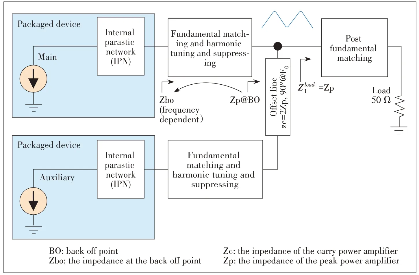
▲Figure 1.Conventional Doherty power amplifier(DPA)design
For packaged power devices,the use of the parasitic de-embedding network to allow waveforms at the intrinsic plane is required.It is crucial when designing a complex power amplifier and investigating its performance.Several approaches were proposed to extract the extrinsic (package)parasitics, as well as the intrinsic parasitics[10-14].A de-embedding network of CGH40010F at 0.9 GHz was presented in Ref.[12].It was derived through a combination of datasheet parameters and the manufacture’s passive packaged models.It has been proved accurate enough at 2.1 GHz,but would result in an unacceptable error at a higher frequency.In Ref.[13], a de-embedding network of CGH40025F was proposed for applications up to 2 GHz.The previous work did not consider the effect of either the feedback capacitance or the inductance due to the gate and drain metallization.At higher frequencies, up to 3 GHz, these effects will impact the de-embedding accuracy.In Ref.[14], the parasitic model was only suitable for narrow bandwidth applications.
This work presents a novel de-embedding technique of packaged GaN transistors, which allows for accurate extraction of the device parasitic.The validation is carried out on a 50 W GaN transistor, which proves the effectiveness of the technique.
2 Proposed De-Embedding Technique
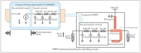
The packaged model of the packaged transistor can be divided into two parts through the de-embedding technique: the frequency independent nonlinear de-embedded intrinsic device (DID)and the frequency dependent linear internal parasitic network (IPN).The IPN can be absorbed into the matching circuit[14-15], as shown in Fig.2.In this way, the design of the PA can be simplified and more accurate.In order to validate the technique,a 50 W GaN transistor is used as a validation in this work.
2.1 Parasitic Network Modeling
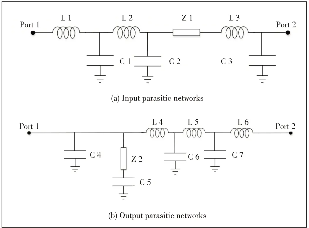
In order to extract the parasitic parameters of a dual-port network, the conventional method assumes that the IPN is completely unknown, and thus it needs to be measured in two cases, namely open and short circuits, as shown in Fig.3a.Measurements should be taken inside the packaged model with special equipment, and Cds, the capacitance between the drain and the source,cannot be calculated.
In this paper, we propose a novel single-port parasitic extraction method as shown in Fig.3b.The parasitic network is modeled by passive components.The reflection coefficient of the external port Γopen is measured with the internal port of IPN open, and the values of components in the IPN model are obtained when Γmod is equal to Γopen.This method requires only external measurements to model a parasitic network without internal measurements.As shown in Fig.4, the input and output parasitic networks of the 50 W GaN transistor are obtained with the proposed technique.The values of the components are listed in Table 1.Fig.5 gives the small signal simulation results of the networks.
2.2 DID Model Calibration
In the proposed de-embedding technique, the parasitic parameter network is obtained through the large signal parametric model simulation.However, the accuracy of IPN is poorer compared with that of DID.In order to improve the accuracy,the model should be calibrated.We can measure the packaged transistor with a precise fixture,and thus an accurate parasitic parameter model is obtained by parasitic parameter modeling.
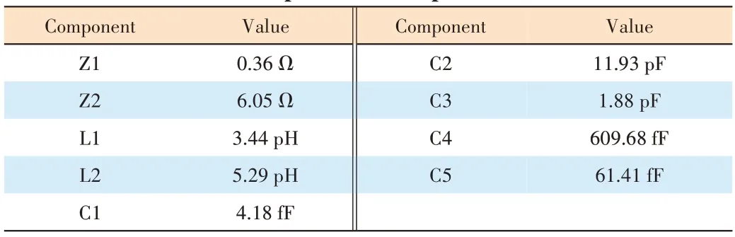
The 50 W GaN transistor is measured using a 6.9 Ω through reflection line (TRL)measurement fixture, as shown in Fig.6.The calibrated accurate parasitic parameter model is shown in Fig.7.The values of the components are listed in Table 2.
2.3 DID Model Verification
▲Figure 2.De-embedding technique of packaged model
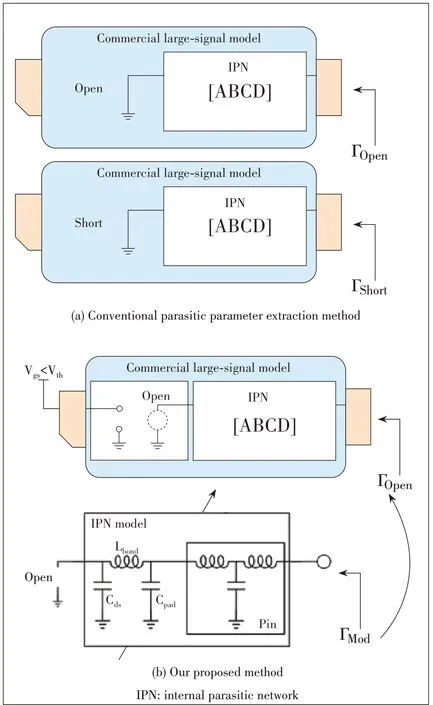
▲Figure 3.Methods to extract parasitic parameters
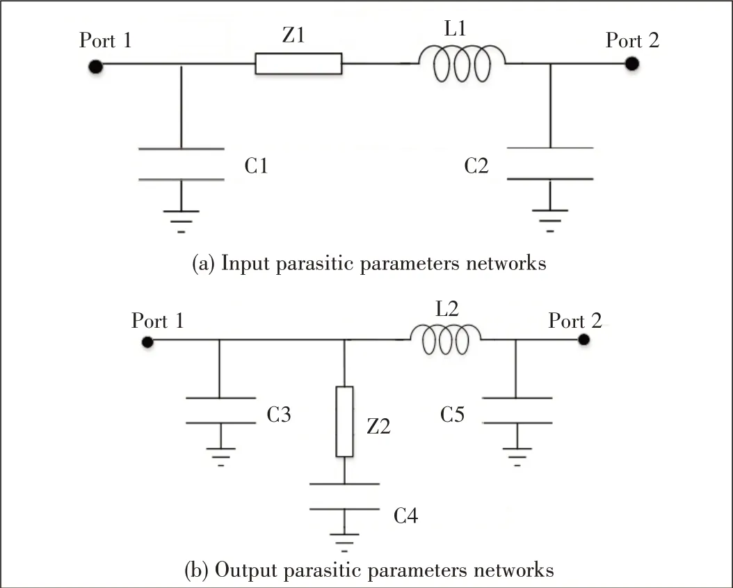
▲Figure 4.Input and output parasitic parameters networks
▼Table 1.Values of the components in the parasitic model
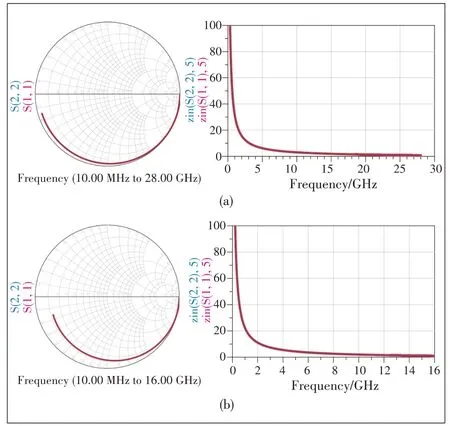
▲Figure 5.Small signal simulation results of(a)the input network and(b)the output network
▲Figure 6.The 6.9 Ω through reflection line(TRL)measurement fixture
According to the parasitic network model, the DID model can be obtained.Considering the DID model is frequency independent, the design of broadband DPA can be significantly simplified.In order to verify the frequency independent characteristics of DID,the DID model of the 50 W GaN power tubes is simulated over a wide frequency range of 500-5 000 MHz.The simulation results are shown in Fig.8.It can be seen from Fig.6 that the output power, efficiency, and gain performance are independent of frequency in the wide frequency range of 500-5 000 MHz.The DID model gives the ideal frequency independent characteristics and the proposed de-embedding technique is confirmed.
3 DPA Design
In order to verify the effectiveness of the de-embedding technique,a broadband Doherty PA using the 50 W GaN transistor is designed and fabricated utilizing the de-embedded model.The demonstrating 200 W DPA is designed at the range of 1.7-2.7 GHz.The fabricated DPA is measured using continuous wave(CW)signals and the measured drain efficiency and power gain are shown in Fig.9.The designed PA exhibits satisfactory power and efficiency performance, which could be a great demonstration of the proposed technique.
▲Figure 7.Calibrated accurate parasitic parameter model
▼Table 2.Values of the components in the calibrated model
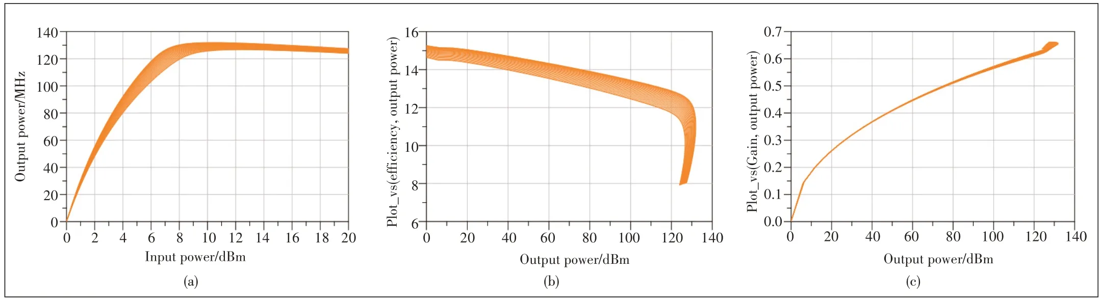
▲Figure 8.Simulation results:(a)output power;(b)efficiency;(c)gain
4 Conclusions
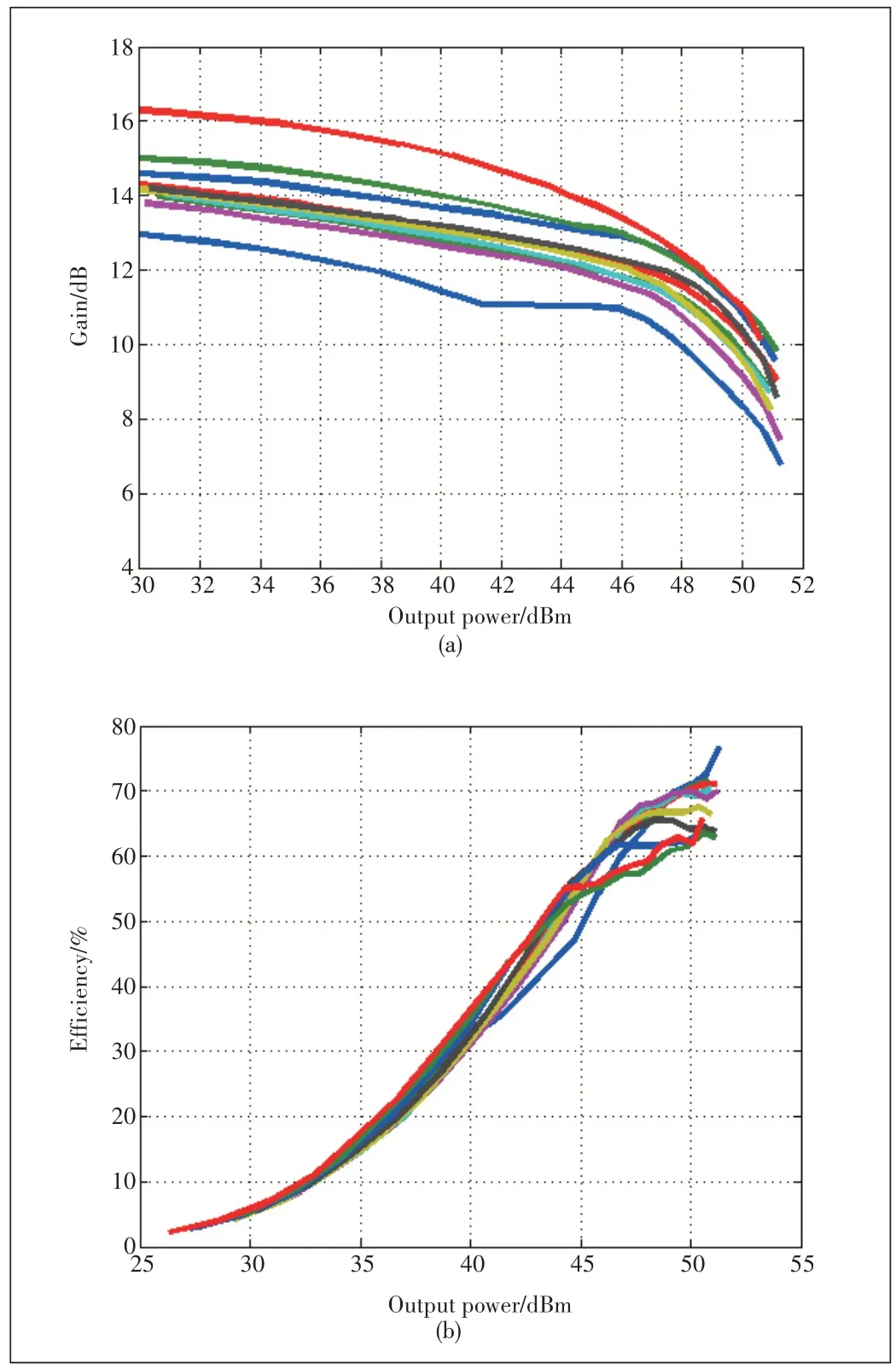
▲Figure 9.Measured(a)drain efficiency and(b)gain of the fabricated DPA
In this paper, a novel de-embedding technique of packaged GaN transistors is proposed and verified.The technique divides the packaged device into the frequency independent DID and frequency dependent IPN, which only requires external measurements.The IPN can be absorbed into the matching circuit,thus the PA design is only based on the DID.Considering the frequency independent characteristic of DID, the method greatly simplifies the design of efficient wideband PA.
Regarding the rationale, this method could be expanded to other packaged microwave power devices.

- ZTE Communications的其它文章
- Editorial:Special Topic on Edge Intelligence for Internet of Things
- Cost-Effective Task Scheduling for Collaborative Cross-Edge Analytics
- Flexible Multiplexing Mechanism for Coexistence of URLLC and EMBB Services in 5G Networks
- Differentially Authorized Deduplication System Based on Blockchain
- Higher Speed Passive Optical Networks for Low Latency Services
- Analysis of Industrial Internet of Things and Digital Twins