Effect of tellurium(Te4+)irradiation on microstructure and associated irradiation-induced hardening*
2021-05-24 02:28:20HefeiHuang黃鶴飛JizhaoLiu劉繼召GuanhongLei雷冠虹OndrejMuranskyTaoWeiandMihailIonescu
Chinese Physics B 2021年5期
Hefei Huang(黃鶴飛), Jizhao Liu(劉繼召), Guanhong Lei(雷冠虹),Ondrej Mur′ansky, Tao Wei, and Mihail Ionescu
1
Shanghai Institute of Applied Physics,Chinese Academy of Sciences,Shanghai 201800,China
2School of Nuclear Science and Technology,University of Chinese Academy of Sciences,Beijing 100049,China
3Australian Nuclear Science and Technology Organisation(ANSTO),Lucas Heights,Sydney,NSW,2234,Australia
4University of New South Wales(UNSW),Kensington,Sydney,NSW,2052,Australia
Keywords: GH3535 alloy,Te ions irradiation,microstructural evolution,irradiation hardening
1. Introduction
The molten salt reactor(MSR)system is one of the generation IV reactors which provides inherent safety(operating at low pressure), high efficiency, and simplified fuel cycle.[1–3]However, the deployment of MSR systems is currently hindered by the availability of structural materials capable of withstanding combination of harsh operating conditions(high temperature,molten salt corrosion,and neutron radiation)for an extended period of time. For instance,the neutron irradiation damage is expected to reach 100 dpa for the core components while the operation temperature is expected to reach of above 750°C.[4,5]
The Ni–Mo–Cr Hastelloy-N alloy developed by Oak Ridge National Laboratory (ORNL) during the Molten-Salt Reactor Experiment (MSRE)[6]in the 60’s is still considered as one of the most promising candidate structural materials for MSR due to its outstanding corrosion resistance.[3]Recently,China has produced a domestic product of the Hastelloy N alloy(GH3535)intended for use in Chine Thorium Molten-Salt Reactor(TMSR).[7]Since,the irradiation damage of these alloys is of paramount importance,a number of researches have used ion irradiation as a surrogate for expected neutrons.[8–11]For instance,in our previous work[12]we showed the temperature effect on the radiation damage in Ni–Mo–Cr(GH3535)alloy weld metal by 8-MeV Ni3+ion irradiation. Similarly,the microstructural changes induced by Xe26+ions irradiation with a dose of up to 10 dpa at different temperatures in GH3535 alloy has been investigated in Ref.[13].
In the present study, we aim to build upon our previous work by using Te4+ions for irradiation. Te is of particular interest in MSR because it is one of the fission products known to cause an embrittlement of Ni-based alloys.[14]GH3535 alloy samples were Te4+ion(15 MeV)irradiated at 650°C.The irradiation hardening and microstructural evolution were then characterized by nano-indentation and transmission electron microscopy (TEM), respectively. The thicknesses of TEM samples were determined by the convergent beam electron diffraction (CBED) method. The thickness of sample S2, S4and S5are about 100 nm and the thickness of sample S3is about 71 nm. The irradiation hardening was also estimated using dispersed barrier hardening(DBH)model based on the TEM micrographs. Moreover, the elements distribution of unirradiated and irradiated samples was characterized by electron probe microanalysis(EPMA).
2. Experimental details
The chemical composition of the studied Ni–Mo–Cr GH3535 alloy is shown in Table 1. Five samples(S1?5)with nominal dimensions of 5 mm×5 mm×1 mm were precisioncut using electrical discharge machining before being progressively polished to the EBSD standards. Samples(S2?5)were then irradiated with 15-MeV Te4+ions at 650°C to the fluence of 2.25×10¹⁴(S2),1.35×1015(S3),4.50×1015(S4),and 9.00×10¹⁵(S5) ions/cm2, respectively. Their peak damages are 0.5 dpa(S2),3.0 dpa(S3),10 dpa(S4),and 20 dpa(S5),respectively, as predicted by SRIM-2013 using Kinchin–Pease Method.[15]Note that S1sample was kept in the unirradiated solution-annealed condition and is used as a reference throughout this paper. Figure 1 shows the Te concentration and dpa profile as a function of depth (the distance from the irradiated surface). Based on SRIM simulations in Fig.1 it is expected that the maximum penetration depth of Te atoms is<3000 nm,while the Te concentration peak is at the depth of about 2250 nm and the peak damage is at the depth of about 1950 nm.

Table 1. The chemical composition of the as-received GH3535 alloy(in unit wt%).

Fig. 1. SRIM predictions of (a) Te atomic concentration and (b) radiationinduced displacement damage for GH3535 alloy at following Te4+ ion fluences: 2.25×1014,1.35×1015,4.50×1015,and 9.00×10¹⁵ ions/cm2.
The Te distribution in the post-irradiated samples was analyzed using the electron probe microanalysis (EPMA, SHIMADZU 1720)while the microstructural evolution was studied using transmission electron microscope(TEM,FEI Tecnai G2 F20). The cross-sectional TEM samples were extracted from perpendicular to the irradiated surface using a focused ion beam (FIB, FEI Helios Nano-lab 600) system with the model of Helios.Lastly,we performed nanoindentation(G200 nanoindenter) in order to infer the radiation-induced hardening of the alloy. The continuous stiffness measurement(CSM)mode was employed to obtain the profile of nanohardness depth dependence.
3. Results and discussion
Figure 2 presents the cross-section Te maps (EPMA) of four samples S1(unirradiated),S3(3 dpa),S4(10 dpa),and S5(20 dpa). No Te atoms(above the background noise)were detected in the S1(unirradiated),S2(0.5 dpa,not shown in Fig.2)and S3(3 dpa) samples. These results suggest that EPMA is not sensitive enough to detect the small amount of Te atoms(Fig.1)in S1and S2samples having Te peak concentration of~35 appm,and ~210 appm,respectively. In the S4(10 dpa,~710 appm)and S5(20 dpa,~1410 appm)samples the layer of increased Te concentration is clearly visible see Figs. 2(c)and 2(d).

Fig. 2. The Te element distribution mappings of (a) the as-received sample and these irradiated samples with irradiated dose of(b)3 dpa,(c)10 dpa,and(d)20 dpa.
However, interestingly the peak Te concentration is detected in the depth of about 2700 nm, while the SRIM predictions shown in Fig.1 suggest the peak Te concentration at the depth of about 2250 nm under the surface. It is believed that the observed discrepancy between the simulations and the observations is caused by the thermal diffusion of Te atoms during high temperature (650°C) irradiation. Note that the SRIM calculation does not take into the account the temperature effect.[15]In addition, the calculation process of SRIM does not consider the cumulative effect of damage.This calculation method assumes that the displacement energy of atoms would not change during the entire irradiation process. In fact,as long as there is local damage,the atoms displace more easily due to looser coupling between the crystal lattices. In other words, the displacement energy of atoms in the irradiation damage region will gradually decrease as the irradiation progresses. Hence, the peak of Te concentration detected by EPMA results is deeper than the SRIM prediction.
The TEM micrograph of the entire irradiation-damage layer of the sample S2(0.5 dpa)is shown in Fig.3(a).It can be seen that the peak damage is located at the depth from about 1800 nm to 2100 nm, which is in agreement with SRIM calculations as shown in Fig. 1. Hence, unlike the depth (position) of the Te peak concentration, the position of the peak damage seems to be unaffected by the temperature. Inserts in Figs.3(b)and 3(c)show TEM micrographs of the peak damage region obtained with the zone-axis close to [011] under the beam condition g = [11ˉ1]. The white dots in Fig. 3(b)(weak-beam dark-field micrograph) become dark in Fig. 3(c)(bright-field micrograph) indicating the formation of dislocation loops, some of the formed dislocation loops are marked by red circles to help the guide the eye.
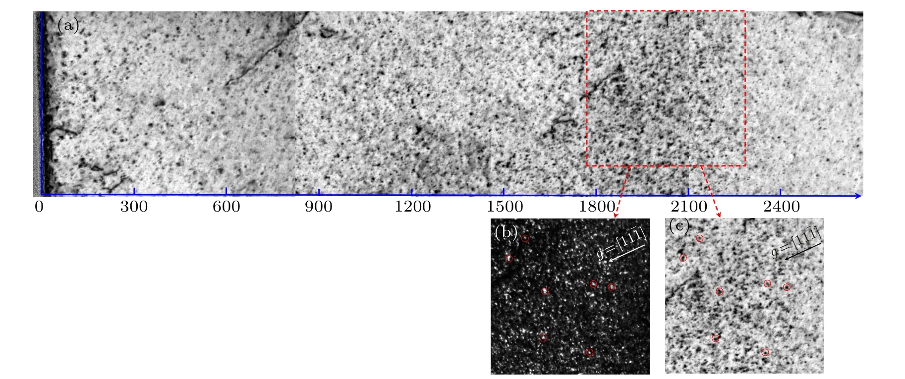
Fig.3. (a)TEM bright-field micrograph of the sample S2 after 15-MeV Te to 0.5 dpa. Weak-beam dark-field(g/3g)micrograph(b)and the corresponding bright-field micrograph(c)showing the formation of dislocation loops.
It is well known that during ion irradiation process, matrix atoms are knocked out from their equilibrium positions by impacting ions, resulting in the formation of interstitials and vacancies.[16]In the process of diffusion, these point defects may encounter each other leading to formation of interstitial and vacancy defect clusters or annihilation of vacancyinterstitial pairs.[17]Formed point defect clusters can then act as embryos for dislocation loops.[18]Compared with vacancytype dislocation loops, interstitial-type dislocation loops are easier to form and grow due to the lower activation energy of migration of interstitial clusters.[19]
Figure 4 shows the bright-field and weak-beam dark-field(g/3g)micrographs of the samples S3(3 dpa),S4(10 dpa),and S5(20 dpa). These micrographs were obtained in the zoneaxis close to[011]under the beam[11ˉ1](g)condition. It can be seen that the number of observed dislocation loops is proportional to the irradiation dose—increasing from S3to S5.In the sample S3(3 dpa)the dislocation loops are relatively dispersed and easily distinguished while in the S4(10 dpa) and S5(20 dpa) samples, cascade collisions led to significantly greater number of dislocation loops which are harder to distinguish. In order to evaluate the size and density of formed dislocation loops we have Nano-Measurer software[12]to analyze collected TEM micrographs.

Table 2. The mean diameters and number densities of dislocation loops in samples S2,S3,S4,and S5.
The mean diameter of formed dislocation loops together with their density are shown in Fig.5 and summarized in Table 2. It became clear that the density of dislocation loops increase with increasing irradiation dose,while their mean diameter is initially increasing with the dose but saturates at 10 dpa reaching about 7 nm. This observation can be explained as follows. In the process of ion irradiation,a concentration gradient of point defects will be established between the position closing to fixed sinks and the position far away from these sinks.[12]The gradient can maintain a flow of point defects towards these sinks to increase the mean diameters of solute clusters or dislocation loops[12]When the defect clusters grow to a certain size,such gradient will disappear. In other words,further ion irradiation will not lead to larger dislocation loops.

Fig.4. TEM micrographs of the samples S3((a1)–(a3)),S4((b1)–(b3)),and S5 ((c1)–(c3)).
It is generally accepted that irradiation defects can pin the movement of dislocations leading to irradiation-induced hardening, which is typically accompanied by the loss of ductility.[20,21]In order to estimate the effect of the irradiationinduced hardening we performed nano-indentation measurement on post-irradiated samples. To ensure that the measured nano-hardness come from different grains, the distance between indentations was set above 80μm(larger than reported grain size[13]). We have performed at least 7 indents on each sample to check the reliability of the measurement.
The typical indentation-depth profiles of the nanohardness measurement are shown in Fig.6. It can be seen that at the indentation depth h >40 nm, nano-hardness decreases with increasing indentation depth. Such depth-dependent nano-hardness behavior is known to be caused by the indentation size effect(ISE).[22]In addition,nano-hardness increases with increasing indentation depth within h <40 nm,which is defined as inverse ISE.[23]The ISE can be explained by Nix–Gao model as the following equations:[24]

where H is the nano-hardness in unit of GPa for a given indentation depth, H0is the nano-hardness at infinite depth in unit of GPa that can be referred to the bulk hardness,h is the indentation depth and h*is a characteristic length which depends on the material and the shape of indenter tip,h and h*are both in units of nm.

Fig.5.(a)The mean diameters and(b)number densities of dislocation loops in samples S2,S3,S4,and S5.

Fig.6.Indentation depth dependence of the nano-hardness in the as-received sample.
Figure 7 presents the average nano-hardness as a function of the indentation depth in the unirradiated(S1)and irradiated(S2,S3,S4,S5)samples. In order to eliminate the uncertainty caused by the surface contamination and complex indenter tip interaction,[25]we have ignored measurements within 100 nm from the surface. Compared with the unirradiated sample,the irradiated samples exhibit clear hardening.It can be also found that the degree of hardening increases with an increasing irradiation dose.It is due to the fact that there are more irradiation defects in the sample under higher ion dose irradiation,which is consistent with results shown in Fig. 5. It has been confirmed that when the indenter presses on the sample surface,a hemispherical plasticity affected region will be formed below the indenter.[26]The radius of this plasticity affected region is approximately 6 to 7 times of the indentation depth.[27]In the other words,the nano-hardness value at a certain depth is the superposition of the nano-hardness of the entire plasticityaffected region. In order to infer the bulk hardness for irradiated materials,Kasada et al. adopted a new method,[28]where the hardness data are plotted as shown in Fig.7(b). The curve for the unirradiated sample shows a good linearity, whereas the curves for irradiated samples seem to have a bilinear character with a shoulder(hc)at about 460 nm. In this study, the critical indentation depth of 460 nm is around 1/7 to 1/6 of the damage layer, which agrees with previous study in Ref.[27].When the indentation depth is beyond the critical indentation depth,a contribution of softer unirradiated region to the measured hardness cannot be neglected. The bilinear behavior in these irradiated samples is due to the softer substrate effects(SSE),which is discussed extensively in Refs.[29,30].
Hence, the bulk hardness can be obtained by the extrapolation of hardness data using the least squares fitting in the range of 100 nm <h for the unirradiated sample and in the range of 100 nm <h <460 nm for the irradiated samples.The H values for samples S1, S2, S3, S4, and S5are 2.42,3.51,3.62,4.56,and 5.00 GPa,respectively. In the study,the nano-hardness increment (ΔH) was defined by the value difference of H0between the irradiated and the unirradiated samples. The calculated values of ΔH for samples S2,S3,S4,and S5are 1.09,1.20,2.14,and 2.58 GPa,as shown in Fig.8. The nano-hardness increments tend to saturate at high nominal ion irradiation dose and follow the following rules:[12]

where ΔH is the nano-hardness increment in unit of GPa,a and b are the fitting parameters. The values of a and b obtained by nonlinear curve fitting are 1.5 and 0.30, respectively. In the previous study,[12]the values of b given by Huang et al. in GH3535 alloy weld metal irradiated by nickel ions is approximately equal to 0.2. This difference may be due to the different microstructure(weld metal versus solution-annealed)and different irradiation conditions, such as type of ions and ion energy.

Fig. 7. Plots of (a) H–h and (b) H2–1/h for the as-received sample and irradiated samples.
The yield strength increment induced by irradiation defects can be estimated using the so-called dispersed barrier hardening(DBH)model[31,32]
where α is the defect barrier strength, M is the Taylor factor (3.06 for fcc metal). For dislocation loops, the value of α should be 0.2.[33]μ is the shear modulus (83.2 GPa), b is the Burgers vector’s module (0.254 nm), N and d are the number densities and mean diameters of dislocation loops.According to Eq. (3), the increments of yield strength for samples S2, S3, S4, and S5are 272.40, 300.46, 427.65, and 476.60 MPa, respectively. The ratio of Δσ among the irradiated samples is 1:1.10:1.57:1.75. Based on the test results of nano-indentation, the ratio of ΔH for the irradiated samples is 1:1.10:1.96:2.37. Taking into account that ΔH is proportional to Δσ,[34]the ratios of ΔH and Δσ among the irradiated samples should be basically the same. In the study, the two ratios are roughly the same, although there are some differences, which are mainly due to the following reasons: In S4and S5samples, the high ion irradiation dose can produce a large number of dislocation loops. These dislocation loops are stacked in a disorderly manner, which brings certain difficulties to statistical work. In addition,there are some very small dislocation loops that were hardly detected by TEM will also contribute to the irradiation hardening.

Fig. 8. The nano-hardness increment versus nominal ion irradiation dose.
4. Conclusion
In the present study,the GH3535 alloy samples were ion irradiated using 15-MeV Te4+at 650°C to a dose of 0.5 dpa(sample S2), 3.0 dpa (sample S3), 10 dpa (sample S4), and 20 dpa (sample S5), respectively. The concentration of implanted Te atoms in post-irradiated conditions was measured using EPMA, while the microstructure evolution was studied using TEM. Finally, we have employed nano-indentation to infer the ion-induced hardening of the studied alloy, respectively. The conclusions can be summarized as follows:
(i) The peak depth positions of the Te peak concentration is underestimated by SRIM calculations, the calculated Te concentration peak is at the depth of 2250 nm, while the EPMA analysis showed that the Te peak concentration is at the depth of about 2700 nm. This discrepancy between the experimental results and SRIM simulations is believed to be caused by thermally driven diffusion of Te atoms.
(ii) It is shown that the Te4+irradiation leads to the formation of dislocation loops. In the process of large ion dose irradiation, the disappearance of the point defects concentration gradient leads to the mean diameter of dislocation loops in samples S4and S5are almost unchanged.
(iii)The ratio of the yield strength increments calculated by DBH model among the irradiated samples is roughly the same as that of the nano-hardness increments measured by nano-indenter. In addition, the 0.3 power law dependence of the nano-hardness increments on dpa is obtained for the GH3535 alloy samples irradiated by Te ions.

- Chinese Physics B的其它文章
- Process modeling gas atomization of close-coupled ring-hole nozzle for 316L stainless steel powder production*
- A 532 nm molecular iodine optical frequency standard based on modulation transfer spectroscopy*
- High-throughput identification of one-dimensional atomic wires and first principles calculations of their electronic states*
- Effect of helium concentration on irradiation damage of Fe-ion irradiated SIMP steel at 300 °C and 450 °C*
- Optical spectroscopy study of damage evolution in 6H-SiC by H+2 implantation*
- Improved 4H-SiC UMOSFET with super-junction shield region*