Preparation of WO3 thin films by dip film-drawing for photoelectrochemical performance☆
2019-08-07 07:54:28DongboXuLiliLiWeiqiangFanFagenWangHongyeBaiBaodongMaoWeidongShi
Dongbo Xu,Lili Li,Weiqiang Fan,Fagen Wang,Hongye Bai,Baodong Mao,Weidong Shi,*
1 School of Energy and Power Engineering,Jiangsu University,Zhenjiang 212013,China
2 School of Chemistry and Chemical Engineering,Jiangsu University,Zhenjiang 212013,China
Keywords:WO3 thin films Dip film-drawing Photoelectrochemical Thicknesses Large-scale
ABSTRACT Here we report the WO3 thin films on F-doped SnO2 conducting glass(FTO)substrates which were prepared by using dip film-drawing method.Dip film-drawing was a simple,convenient,economical method and in largescale to prepare photoanodes for future applications.The FTO substrates were dipped in tungstic acid solution then film-drawn included 3, 6, 9, 12 and 15 times for prepared different thicknesses of WO3 thin film photoanodes. Then the photoanodes were employed as the electrodes in photoelectrochemical property measurements,which include scan linear sweep,repeated on/off illumination cycles,electrochemical impedance spectroscopy and incident photon to current conversion efficiency,respectively.The results showed that the WO3 thin films dipped 9 times with 175 nm thicknesses had the best photoelectrochemical performance of 0.067 mA·cm-2 at 1.23 V versus RHE.
1.Introduction
Hydrogen as an ideal green energy can be produced by photoelectrochemistry(PEC)using semiconductor photoelectrodes for water splitting which is an environmentally friendly method [1-5].Among semiconductors, WO3with small bandgap (Eg? 2.6 eV) has attracted extensive attention for a kind of electrochromic and photoelectrode material[6-10].For example,there are many reports about WO3as photoelectrodes for water splitting, Su et al. reported WO3nanowire and nanoflake arrays for PEC water oxidation,in which the morphology of WO3plays an important role in PEC performance[11]. Wang et al. reported WO3nanoflakes by hydrogen treatment which show enhanced photostability[12].Moreover,Park et al.also reported WO3thin films prepared by dip coating for electrochromic and photoelectrochromic devices[13].Meanwhile,for preparing WO3thin films,various fabrication methods including sputtering[14],hydrothermal treatment[15],sol-gel[16,17],vacuum evaporation[18],electrophoresis[19],and electrospinning[20],have been proposed.However,the sputtering and vacuum evaporation methods needed expensive equipment and the hydrothermal,electrophoresis and electrospinning methods could not prepare WO3thin films in large-scale for application.Therefore,it is still a challenge to find an economical method for preparing WO3thin films in large-scale.
In recent years,the dip film-drawing method as a kind of simple,convenient,economical,and environmentally benign method which can be performed in large-scale for preparing thin films has attracted a great deal of attention.What's more,dip film-drawing method in fact is a simple method for preparing a uniform thin film on a substrate [21-24].However,using the dip film-drawing method for preparing WO3thin films is still an urgent need to address the thicknesses of WO3thin films and regard the photoelectrochromic activity of the thin films.
In this work, we prepared WO3thin films on fluorine-doped tin oxide(FTO)substrates by using a fully automatic dip film-drawing instrument.The WO3thin films were prepared by dipping the FTO substrate into tungstic acid (H2WO6)solution, keeping it for some time and then drawing it up,making one cycle(see the Experimental section).For different thicknesses of WO3thin films,the process recycled different times.Finally,the WO3thin films as photoanodes were used for assessing the effects of photoelectrochemical properties reported in here by the scan linear sweep(LSV),repeated on/off illumination cycles(I-t)and electrochemical impedance spectroscopy(ESI)measured.Incident photon to current conversion efficiency(IPCE)was also implemented in this system that occurs in the different thicknesses of WO3thin films as a function. Thereby, according to these measurements,we can understand that the thicknesses of the films in prepared samples were a key factor with the best photoelectrocatalytic activity.
2.Experimental
2.1.Preparation of the WO3 thin flims
The WO3thin films were synthesized by simple dip film-drawing and annealing methods.In traditional,20 ml of 30%hydrogen peroxide solution was added into 0.5 g of tungstic acid (H2WO6) powder in a 50 ml beaker.Then the mixing precursor solution was ultrasonically dispersed and continuously stirred for 2 h to yield a pale yellow transparent solution.The 3 cm×1.5 cm sized F-doped SnO2conducting glass(FTO)substrates were cleaned by ethanol,acetone,and distilled water in an ultrasonic bath for 20 min, respectively. Then, the FTO glasses were dipped into the pale yellow transparent solution for 60 s by using a dip film-drawing instrument, and their film-drawing rates with up and down were 1000 μm·s-1.The FTO substrates were dipped included 3,6,9,12 and 15 times and the interval time was 180 s for dip film-drawing every time with the temperature of 30°C in the system all the time then obtained H2WO6films on the surface of FTO substrates.The obtained H2WO6thin films were annealed in air at 500°C for 2 h to form WO3thin films. Finally, the samples of FTO substrates with WO3thin films were denoted as 3-WO3,6-WO3,9-WO3,12-WO3and 15-WO3,respectively.
2.2.Structural and morphology characterization
The structure of the WO3thin films was analyzed by the powder X-ray diffraction patterns (XRD, Bruker D8 ADVANCE X-ray diffractometer)with the scanning rate of 7.0(°)·min-1from 10°to 70°.The morphology was studied using a scanning electron microscope(SEM,Hitachi S-4800).The diffuse reflection spectra(DRS)of the samples were recorded on a UV-visible spectrophotometer(Shimadzu UV-3100,Japan)with BaSO4as the reflectance standard.
2.3.Photoelectrochemical measurements
Photoelectrochemical(PEC)properties of the thin films were measured in a three-electrode electrochemical cell with 0.5 mol·L-1Na2SO4in PEC while Pt wire,Ag/AgCl,and as-prepared WO3thin films coated on FTO/glass were used as counter,reference,and working electrodes,respectively.The samples with an area of 1 cm2were exposed up on simulated sunlight irradiation at 50 mW·cm-2(AM 1.5 G)provided by a 300 W xenon lamp.The scan linear sweep(LSV),repeated on/off illumination cycles(I-t)and electrochemical impedance spectroscopy(ESI)were implemented through an electrochemical workstation(CH Instruments,CHI-760),respectively.Incident photon to current conversion efficiency(IPCE)was measured by an external quantum efficiency measurement system (Newport/Oriel, QE-PV-SI) connected with an electrochemical work-station.
3.Results and Discussion
XRD analysis was employed to characterize the crystalline phases of the WO3powder by scraping the 9-WO3thin films from FTO substrates.As shown in Fig.1,the diffraction peaks of WO3are corresponding to the standard card JCPDS No.75-2072 of WO3[25].
To examine the detailed morphology and microstructure of the WO3thin film photoanodes, SEM images were carried out. As shown in Fig. 2(a)-(c), top-view SEM images of 3-WO3, 6-WO3,and 9-WO3thin films show a slight agglomeration and without any apparent voids. Simultaneously, with the dipped film-drawing times sequentially added, the 12-WO3and 15-WO3thin films(Fig. 2(d), (e)) are changed to granules with uneven size, and the WO3further assembled as compact films.The reason for this result is that with the dipped film-drawing times added, the H2WO6thin films on the surface of FTO are unstable in the thermodynamic system and then after the high temperature anneal, the WO3thin films appeared uneven and compact thin films.

Fig. 1. XRD patterns of the WO3 powder by scraping the 9-WO3 thin films from FTO substrates.
To examine the thicknesses of WO3thin films,the SEM images of cross profile were shown in Fig.3.It clearly can be seen that at 3 times of dipped film-drawing, the 3-WO3thin films were uneven and ultrathin on the surface of FTO.When the dipped film-drawing times were 9 times, the thicknesses of 9-WO3thin films in Fig. 3(b) were approximate 175 nm. In addition, as shown in Fig. 3(c), when the dipped film-drawing times were 15 times,the thicknesses of 15-WO3thin films were about 425 nm. Thus, it is evident that as the dipped film-drawing times gradually increase, the thin film thicknesses of WO3also increase.
According to the UV-vis optical absorption spectra in Fig.4,it can be observed that the pure FTO shows no significant influence on the ability of light absorption.However,the WO3thin films exhibit substantially better optical properties from 200 nm to 500 nm.Apparently,it should be pointed out that with the thicknesses of WO3thin films added,the UV-vis optical absorption was also gradually changed to become stronger.This result clearly indicated that the thicknesses of WO3thin films would have decided the optical absorption in PEC process.
Linear-sweep-voltammetry(LSV),as shown in Fig.5,with a scan rate of 0.05 V·s-1was used to detect photoelectrochemical properties of asprepared WO3thin film photoanodes.The black line was in dark and it clearly can be seen that the photocurrent density was negligible than the photoresponse of WO3thin film photoanodes under light irradiation indicating that all the photocurrents come from the photoelectric conversion.The 9-WO3thin films display the maximum photoresponse activity with a photocurrent density of 0.067 mA·cm-2at 1.23 V versus RHE.In contrast,the 3-WO3,6-WO3,12-WO3and 15-WO3thin films display the photocurrent density of 0.042 mA·cm-2, 0.048 mA·cm-2,0.059 mA·cm-2and 0.049 mA·cm-2at 1.23 V versus RHE,respectively.Prominently, the best thicknesses of WO3thin films are 175 nm for dipped film-drawing 9 times.The reason for this result is that when the dipped film-drawing time was less than 9 times,the thicknesses of WO3thin films are uneven and ultrathin(Fig.3)so the absorption of light for WO3thin films is weak when dipped less than 9 times.However,when the dipped film-drawing time was more than 9 times, the WO3thin films show a strong absorption for light but the photocurrent densities are lower.The reason can be attributed to that the 12-WO3and 15-WO3thin films enhanced the distance between WO3surface and FTO substrate,so the interfacial charge was greatly recombined before transfer to the FTO. Therefore, the best times for dipped film-drawing of WO3thin films were 9 times and the thicknesses were 175 nm.
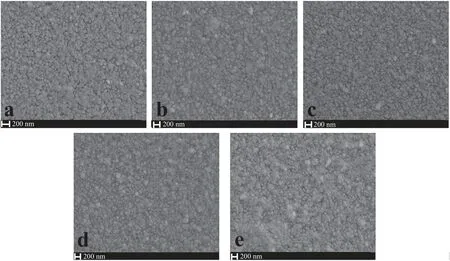
Fig.2.Top-view SEM images of WO3 films:(a)3-WO3;(b)6-WO3;(c)9-WO3;(d)12-WO3;(e)15-WO3.

Fig.3.Cross profile SEM images of WO3 films:(a)3-WO3;(b)9-WO3;(c)15-WO3.
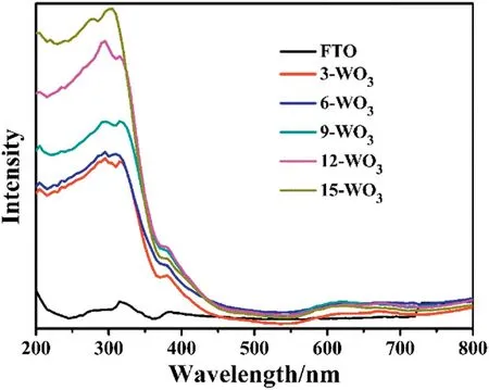
Fig.4.UV-vis optical absorption spectra of WO3 thin films.
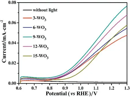
Fig.5.LSV characteristic curves of WO3 thin film samples measured in the illumination and dark.
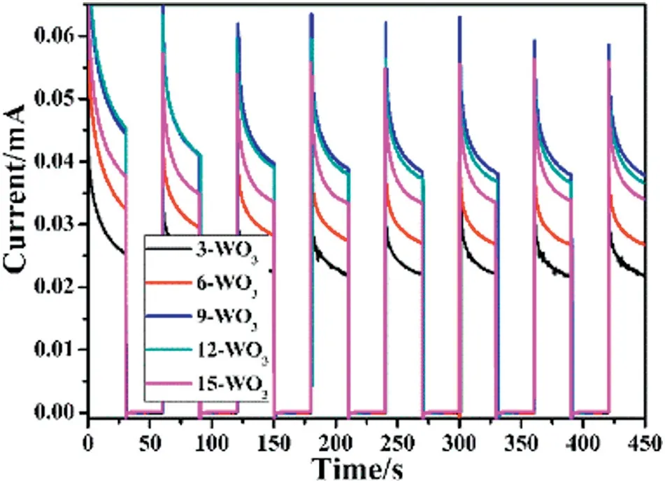
Fig.6.I-t curves of different WO3 samples measured with applied potential of 0.5 V vs Ag/AgCl in the simulated solar light.
Similarly,the I-t curves(Fig.6)of repeated on/off illumination cycles were measured which were performed in order to check the stability of the WO3thin film photoanodes and with switching on the irradiation,it revealed that the photocurrent rapidly rises depending on the thicknesses of the WO3thin films.Moreover,the 9-WO3thin films have the strongest photocurrent in 450 s which was in good agreement with the LSV result.At the same time,the long-term stability of 9-WO3thin films was employed at 1.23 V versus RHE.As shown in Fig.7,the overall photocurrent density decreases a little after 6 h.The result suggests that the WO3thin films have good response ability for light and chemical stability in PEC measurements as a promising photoanode for future applications.

Fig. 7. I-t curves of 9-WO3 thin films for stability measured of 1.23 V vs RHE in the simulated solar light.
In order to investigate the charge transport behavior of WO3thin film photoanodes, electrochemical impedance spectra (EIS) studies were performed. The EIS was measured in a 0.5 mol·L-1Na2SO4solution under the simulated solar light with 50 mW·cm-2in a threeelectrode system. The frequency was from 1 Hz (low frequency) to 105Hz(high frequency).Normally, in the high-frequency range, the radius of semicircle was proportional to the resistance and the larger semicircle means the stronger resistance.As shown in Fig.8,the 9-WO3thin films exhibit the smallest radius of arc, indicating that the EIS was the lowest so that the charge transfers the fastest in the 9-WO3thin films. These are highly consistent with the LSV and I-t results.
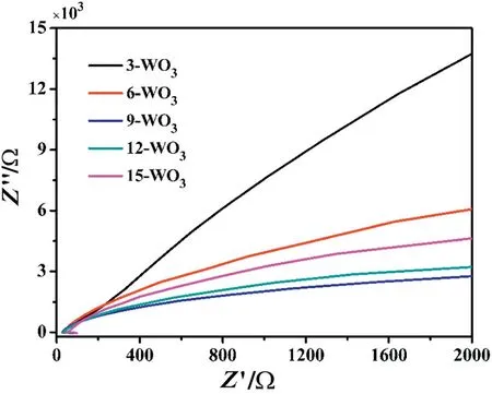
Fig.8.EIS studies of WO3 thin films in the simulated solar light.
The IPCE was employed in a three-electrode photoelectrochemical system to understand the relationship between the electrochemical activity and light absorption.As shown in Fig.9,the IPCE of WO3thin films was obtained by the equation[26-29]:


Fig.9.IPCE spectra of different WO3 thin films measured in 0.5 mol·L-1 Na2SO4 solution at a voltage of 0.6 V vs Ag/AgCl.
where I (mA·cm-2) is the photocurrent density at specific incident wavelengths, λ (nm) is the wavelength of incident light, and Jlight(mW·cm-2) is the power density of the incident light.The IPCE of the 9-WO3thin films has the maximum value about 24%at 340 nm wavelength; 9-WO3thin film has better IPCE values than the other WO3thin films from 300 nm to 500 nm wavelength.The IPCE results are exactly consistent with the LSV,EIS and I-t results.It is noteworthy that the highest IPCE value could be attributed to the best thicknesses of 9-WO3thin films which have the best charge transfer distance, the highest charge separation efficiency and satisfactory electrical conductivity.
4.Conclusions
In summary,a kind of WO3thin film photoelectrode has been successfully synthesized on FTO substrates by simple dip film-drawing and annealing methods. The structure, morphology and thicknesses of the WO3thin films were analyzed by XRD and SEM. The photoelectrochemical performances were studied by LSV,I-t,EIS and IPCE.The results show that the 9-WO3thin films with 175 nm thicknesses have the best PEC performance which was attributed to the best charge transfer distance from the WO3thin film surface to the FTO.
 Chinese Journal of Chemical Engineering2019年5期
- Chinese Journal of Chemical Engineering的其它文章
- Synthesis of high purity Li2CO3 and MgCO3·3H2O in a homogeneous-like organic phase☆
- Impact of recycling improvement on the life cycle of phosphorus
- Methane hydrate formation and dissociation behaviors in montmorillonite☆
- Flux mechanism of compound flux on ash and slag of coal with high ash melting temperature☆
- An energy saving and fluorine-free electrorefining process for ultrahigh purity lead refining☆
- Mineral phase and structure changes during roasting of fine-grained carbonaceous gold ores and their effects on gold leaching efficiency☆