結(jié)晶性和粒子尺寸對C60薄膜晶體管遷移率的影響
2018-03-14 06:35:27孫志鵬馬延文
無機化學(xué)學(xué)報 2018年3期
關(guān)鍵詞:南京
李 誼 韓 笑 孫志鵬 馬延文
(南京郵電大學(xué)材料科學(xué)與工程學(xué)院,南京 210023)
0 Introduction
In recent decades,organic thin film transistors(OTFTs)have received considerable attention owing to their low cost,low temperature process,compatibility with plastic substrate,and wide potential applications in large-area,lightweight,flexible electronics devices such as electronic displays,organic memories,and sensors[1-5].Much research work has been focused on obtaining high performance OTFTs comparable to those of amorphous silicon thin film transistors (TFTs)[6-10].In addition to the optimization of device structure and performance,the correlation of the charge transport with the thin-film microstructure hasalso been extensively studied.It is well known that the charge transfer in OTFTs highly rely on the crystallinity,molecular ordering and crystal grain sizes,which in turn depend on the molecular structures of the organic semiconductors[11-12],deposition process[13-16],and substrates[17-18].For the most planar organic semiconducrors molecules,such as CuPc,F16CuPc,pentacene,perylene bisimide and oligothiophene,increasing substrate temperature (Ts), decreasing deposition rate, and incre-asing deposition pressure in vacuum deposition process normally leads to a highly ordered film with larger grain sizes and fewer grain boundaries,which is regarded as the most effective way to obtain highmobility devices[14-25].However,for the spherical C60semiconductor,which is an important n-type semiconductor material with high mobility,the mechanism of charge transport in C60films is still unclear,and the relationship between mobility and microstructure of the C60films is controversial[20,26-28].Therefore,it is essential to investigate the effect of morphology and structure,which are quite sensitive to growth conditions,on the performance of the C60films in-depth.In this study,the crystallinity and grain size of the C60films have been regulated by changing the Tsand deposition pressure in the vacuum deposition process.X-ray diffraction (XRD)and atomic force microscopy(AFM)were used to investigate the morphology and crystalline structure of thin films.Furthermore,the mobilities of the films are obtained by field-effect measurements,and the correlations of mobility with crystallinity and grain size of the C60films are established.
1 Experimental
1.1 Fabrication of C60TFTs
Fig.1 showsthe schematic diagram ofthe fabricated C60TFTs.C60(99.9%)is purchased from Aldrich and used without further purification.The substrate is 300 nm SiO2thermally grown on a heavily doped n-Si wafer,which were ultrasonically cleaned with acetone,isopropyl alcohol,and ultrapurified water,successively.A bottom-gate,top-contact device configuration of C60TFTs was adopted.First,the substrate was set in the chamber and maintained at 4×10⁻⁵Pa.Subsequently,a 40 nm thick C60active layer[16],patterned through a shadow mask,was deposited by vacuum evaporation onto the substrate under a specific Ts(i.e.,30,60,90,130,160 and 190 ℃)at the same rate of 0.01 nm·s-1recorded by a quartz crystal oscillator.Finally,the gold (Au,99.99% )electrodes,with a thickness of 50 nm,were defined on the C60film by thermal evaporation through another mask.For the samples of different deposition pressure,the films were deposited by vacuum deposition under a specific Pdep(i.e.1×10-4and 1×10⁻¹Pa)with the rate of 0.01 nm·s-1and the Tsof 130℃.The channel length (L)and width (W)are 70 and 500 μm,respectively.
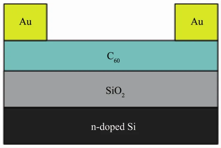
Fig.1 Schematic diagram of the fabricated C60TFTs
1.2 Charcterization
The structures and surface morphologies of the films were characterized by X-ray diffraction(XRD,Philips X′pert Pro X-ray diffractometer in 2θ range of 15°~28°,Cu Kα1radiation of 0.154 nm)and atomic force microscopy (AFM,Bruker Dimension Icon,tapping Mode).The performances of the devices were evaluated by semiconductor characterization system(Keithley model 4200-SCS)under vacuum condition at room temperature.
2 Results and discussion
2.1 Surface morphology and structure of C60 films
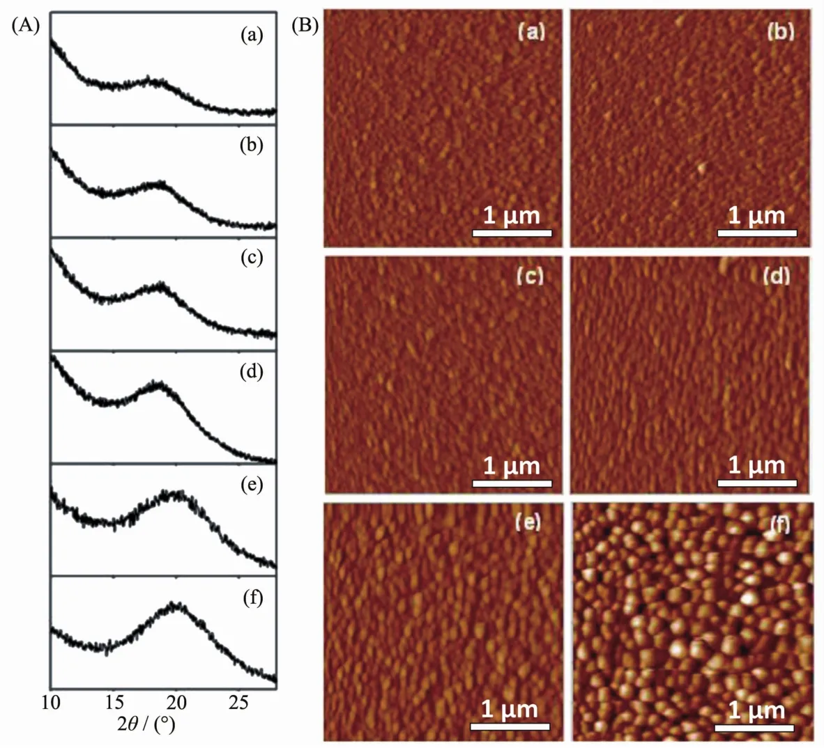
Fig.2 Characteristic XRD patterns (A)and AFM images (B)of the 40 nm C60films deposited under different Tsof 30,60,90,130,160 and 190 ℃ (a~f),respectively
The characteristic XRD patterns and morphologies of the C60films deposited under different Tsare shown in Fig.2.The XRD patterns of the C60films show broadened (113)peaks,corresponding to the D values of ca.1.54 nm.With increasing Tsfrom 30 to 190 ℃,the intensity of(113)peaks increase,indicating the increased crystallinity of the films (Fig.2A).The morphological evolutions of the C60films with Tsare demonstrated in Fig.2B.It is clearly seen,the grain sizes keep almost unchanged for Tsbelow 90℃(Fig.2B(a~c)),and gradually increase for further increasing Tsfrom 90 to 190 ℃ (Fig.2B(d~f)).The root-meansquare roughness of all the samples obtained from the AFM measurements are about 1~3 nm,indicating the smooth surfaces of the films.
2.2 Electronic properties of C60films
Fig.3 shows the output characteristics of C60TFTs prepared under different Ts.The C60TFTs exhibit typical n-channel field-effect behavior,operated under a positive voltage source-drain voltage (Vd)and gate voltage (Vg),with distinct linear and saturation regions in the output curves.With increasing Tsfrom 30 to 130℃,a significant increase of saturation drain current(Id)from 1.8 to 12.3 μA is observed when they are biased at Vd=60 V and Vg=60 V (Fig.3a~d).With further increasing Tsto 160 and 190℃,Iddecreases to 4.2 μA and 2.1 μA,respectively.
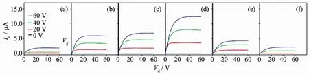
Fig.3 Output(Id-Vd)characteristics of C60TFTs prepared under different Tsof 30,60,90,130,160 and 190 ℃ (a~f)

Fig.4 Transfer (Id-Vg)characteristics of C60TFTs prepared under different Tsof 30,60,90,130,160 and 190℃
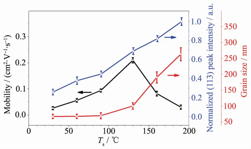
Fig.5 Carrier mobilities,grain sizes,and crystallinity((113)peak intensity)of C60thin films as functions of Ts
Fig.4 shows the transfer characteristics of C60TFTs prepared under different Ts.From the transfer curves,the carrier mobility are extracted for each device,and the relationship between the mobilities and Tsare shown in Fig.6.In order to make clear of the correlation of the mobilities with the corresponding crystallinity and morphologies of the C60films,the changes of(113)peak intensity and grain sizes with Tsare re-plotted here.It is seen that,for C60films with Tsbelow 130℃,the mobilities increase from 0.026 to 0.211 cm2·V-1·s-1with increasing Ts.With further increasing Tsto 160 and 190℃,mobilities decrease to 0.082 and 0.030 cm2·V-1·s-1,respectively.Because of the unchanged grain sizes of C60films deposited under 30,60 and 90℃,the increase of mobilities could be attributed to the increased crystallinities of films.When Tsis up to 130℃,the larger mobility was achieved mainly due to the higher crystallinities despite the slightly increased grain sizes.Interestingly,for the films with Tsof 160 and 190℃,despite the increases in the crystallinities,remarkable decreased mobilities are obtained,which should be related the obviously increased grain sizes.These results suggest the different grain-boundary effect for the spherical C60molecules from that for the planar molecules,such as CuPc,pentacene,TIPS-pentacene,perylene bisimide and oligothiophene[14-25].For the planar molecules,the grain boundary is a crucial barrier for the carrier transport,since the intermolecular charge hopping across the grain boundaries is less efficient than that within the grains.Thus,reducing the grain boundaries by increasing grain sizes is a promising approach to improve charge transport and mobility.However,for the C60samples with Tsof 160 and 190℃,the larger grain sizes of spherical C60films lead to the lower mobilitis,which isinterestingand worth further investigating.
In order to reveal the influence of grain sizes on the mobilities of C60films,the samples with similar crystallinities and different grain sizes are needed.In our previous study,we have demonstrated that higher deposition pressure in vacuum deposition could lead to the larger grain sizes of C60films with unchanged crystallinities and molecular packing[16].Thus,the C60films with deposition pressure of 1×10⁻¹Pa and Tsof 130℃are deposited and investigated.In contrast to the C60films with deposition pressure of 1×10⁻⁴Pa(Fig.2Ad and 2Bd),the samples of 1×10⁻¹Pa show the unchanged crystallinities and increased grain sizes,as shown in Fig.6.The C60films with deposition pressure of 1 ×10⁻¹Pa have a mobility of 0.030 cm2·V-1·s-1,which is lower than the value of samples with deposition pressure of 1×10⁻⁴Pa.Due to the unchanged crystallinities,the decrease ofmobility should be corrected to the increased grain size.
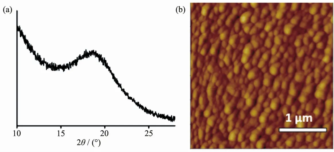
Fig.6 Characteristic XRD pattern (a)and AFM image (b)of the 40 nm C60films deposited under 1×10⁻¹Pa and 130 ℃
As known,the performance ofOTFTs is determined by the crystalline order and grain sizes of the first few molecular layers of the semiconductor near the semiconductor/dielectric interface. To ascertain the grain sizes of the C60layers at C60/SiO2interface,two C60films of 10 nm thickness were deposited on SiO2at deposition pressure of 1×10⁻⁴and 1×10⁻¹Pa,respectively.From the corresponding AFM images in Fig.7a and b,it is seen that,the 10 nm C60films deposited under 1×10⁻⁴Pa have a lot of small grains,while some larger grains are observed for the films of 1×10⁻¹Pa.This confirmed that larger grain sizes of C60films result in the lower mobilities.The possible mechanism for the effect of grain size on mobility of C60films is proposed in Fig.7c and d.For the spherical C60molecules,carrier could be effectively transported through nearest-neighbor hopping between molecules[26].So the films with small and close grains are advantageous to effective charge transport(Fig.7c).For the films with large grain size,it is difficult to realize the nearest-neighbor hopping between grains molecules,due to the large spacing between the grains (Fig.7d).Thus,the grain boundary is not a serious barrier for the charge transport,and the larger grain size could lead to the lower mobility in C60TFTs.
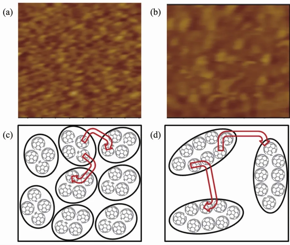
Fig.7 AFM images of 10 nm C60films deposited under(a)1×10⁻⁴and (b)1×10⁻¹Pa,and the possible charge transfer mechanism of C60films with different grain size (c,d)
3 Conclusions
In summary,C60films have been prepared on SiO2substrates by vacuum deposition under different substrate temperature ranging from ranging from 30 to 190 ℃ and deposition pressure of 1×10⁻⁴and 1×10⁻¹Pa.The experimentalresults indicate thatthe crystallinity and grain size of the C60films thereof the mobility of the obtained TFTs could be effectively regulated by tuning substrate temperature and deposition pressure.A clear correlation of mobility with crystallinity and grain size ofthe C60film is established.It is found that,both the crystallinity and the grain size of the C60films increase with increasing substrate temperature.And the grain sizes of the films increase and the crystallinity keep almost unchanged with increasing deposition pressure.The mobilities of the C60films are closely correlated with the crystallinity and grain size.The increased crystallinity of the C60films gives the improved mobility.Different from the films of planar organic semiconducrors molecules,for the spherical C60molecules films,the larger grain size could lead to the lower mobility.This study is helpful for the understanding of the charge transfer process and improving the performance of OTFTs.
[1]Someya T,Bao Z,Malliaras G G.Nature,2016,540:379-385
[2]Nomura K,Ohta H,Takagi A,et al.Nature,2004,432:488-492
[3]Baeg K,Khim D,Kim J,et al.Adv.Funct.Mater.,2012,22:2915-2926
[4]Someya T,Sekitani T,Iba S,et al.Proc.Natl.Acad.Sci.USA,2004,101:9966-9970
[5]Rotzoll R,Mohapatra S,Olariu V,et al.Appl.Phys.Lett.,2006,88:123502
[6]Li Y,Liu Q,Wang X Z,et al.Sci.China.Tech.Sci.,2012,55:417-420
[7]Sun X,Zhang L,Di C,et al.Adv.Mater.,2011,23:3128-3133
[8]Virkar A,Mannsfeld S,Toney M F,et al.Adv.Funct.Mater.,2009,19:1962-1970
[9]LI Yi(李誼),LIU Qi(劉琪),CAI Jing(蔡婧),et al.Chinese J.Inorg.Chem.(無機化學(xué)學(xué)報),2014,11:2621-2625
[10]Kelley T W,Boardman L D,Dunbar T D,et al.J.Phys.Chem.B,2003,107:5877-5881
[11]Facchetti A,Letizia J,Yoon M H,et al.Chem.Mater.,2004,16:4715-4727
[12]Zhang X R,Richter L J,DeLongchamp D M,et al.J.Am.Chem.Soc.,2011,133:15073-15084
[13]Li L,Hu W,Fuchs H,et al.Adv.Energy Mater.,2011,1:188-193
[14]Bao Z,Lovinger A J,Dodabalapur A.Adv.Mater.,1997,9:42-44
[15]Horowitz G,Hajlaoui M E.Adv.Mater.,2000,12:1046-1050
[16]Li Y,Chen S,Liu Q,et al.J.Phys.Chem.C,2012,116:4287-4292
[17]Yang S Y,Shin K,Park C E.Adv.Funct.Mater.,2005,15:1806-1814
[18]Br?uer B,Kukreja R,Virkar A,et al.Org.Electron.,2011,12:1936-1942
[19]Ye R,Baba M,Ohishi Y,et al.Mol.Cryst.Liq.Cryst.,2006,444:203-210
[20]Li Y,Chen S,Liu Q,et al.J.Phys.Chem.C,2014,118:14218-14226
[21]Hu Y,Qi Q,Jiang C.Appl.Phys.Lett.,2010,96:133311
[22]Schmidt R,Oh J H,Sun Y S,et al.J.Am.Chem.Soc.,2009,131:6215-6228
[23]Acton O,Ting G G,Shamberger P J,et al.ACS Appl.Mater.Interfaces,2010,2:511-520
[24]Yakuphanoglu F,Gunduz B.Synth.Met.,2012,162:1210-1239
[25]Chen J,Tee C K,Shtein M,et al.J.Appl.Phys.,2008,103:114513
[26]Sung C,Kekuda D,Chu L F,et al.Adv.Mater.,2009,21:4845-4849
[27]Kobayashi S,Takenobu T,Mori S,et al.Sci.Technol.Adv.Mater.,2003,4:371-375
[28]Anthopoulos T D,Singh B,Marjanovic N,et al.Appl.Phys.Lett.,2006,89:213504
猜你喜歡
中國自動識別技術(shù)(2023年6期)2024-01-12 08:13:22
環(huán)球時報(2022-08-16)2022-08-16 15:13:53
兒童故事畫報(2020年8期)2020-10-30 01:58:28
學(xué)生天地(2020年31期)2020-06-01 02:32:22
金色年華(2017年8期)2017-06-21 09:35:27
金色年華(2017年7期)2017-06-21 09:27:54
電影(2017年1期)2017-06-15 16:28:04
中國化肥信息(2016年41期)2016-05-17 04:25:59
新高考·英語進(jìn)階(高二高三)(2016年1期)2016-03-05 09:05:18
連環(huán)畫報(2015年8期)2015-12-04 11:29:31