Initial growth and microstructure feature of Ag films prepared by very-high-frequency magnetron sputtering?
2017-08-30 08:26:08YueZhang張悅ChaoYe葉超XiangYingWang王響英PeiFangYang楊培芳JiaMinGuo郭佳敏andSuZhang張蘇
Chinese Physics B 2017年9期
Yue Zhang(張悅),Chao Ye(葉超),2,?,Xiang-Ying Wang(王響英), Pei-Fang Yang(楊培芳),Jia-Min Guo(郭佳敏),and Su Zhang(張蘇)
1 College of Physics,Optoelectronics and Energy,Soochow University,Suzhou 215006,China
2 Key Laboratory of Thin Films of Jiangsu Province,Soochow University,Suzhou 215006,China
3 Medical College,Soochow University,Suzhou 215123,China
Initial growth and microstructure feature of Ag films prepared by very-high-frequency magnetron sputtering?
Yue Zhang(張悅)1,Chao Ye(葉超)1,2,?,Xiang-Ying Wang(王響英)3, Pei-Fang Yang(楊培芳)1,Jia-Min Guo(郭佳敏)1,and Su Zhang(張蘇)3
1 College of Physics,Optoelectronics and Energy,Soochow University,Suzhou 215006,China
2 Key Laboratory of Thin Films of Jiangsu Province,Soochow University,Suzhou 215006,China
3 Medical College,Soochow University,Suzhou 215123,China
The initial growth and microstructure feature of Ag films formation were investigated,which were prepared by using the very-high-frequency(VHF)(60 MHz)magnetron sputtering.Because of the moderate energy and very low flux density of ions impinging on the substrate,the evolutions of initial growth for Ag films formation were well controlled by varying the sputtering power.It was found that the initial growth of Ag films followed the island(Volmer—Weber,VW)growth mode,but before the island nucleation,the adsorption of Ag nanoparticles and the formation of Ag clusters dominated the growth.Therefore,the whole initial stages of Ag films formation included the adsorption of nanoparticles,the formation of clusters,the nucleation by the nanoparticles and clusters simultaneously,the islands formation,and the coalescence of islands.
Ag film,initial growth,very-high-frequency sputtering
1.Introduction
Recently,the Ag thin films and nanostructures have been paid more attention because of their unique optical and electrical properties,[1,2]a strong coupling of surface plasmons with the incident light,[3,4]and the application as the substrate for silicene epitaxial growth.[5–7]These applications are highly sensitive to the subtle difference in their shape,size,and distribution,thus the morphology of Ag thin films and nanostructures strongly govern these properties.Because the initial formation stages set the characteristic length scales during growth of Ag thin films from the vapor phase,they are decisive for the morphological and microstructural features of Agfilms and nanostructures.
The initial stages of Ag films formation have been well investigated for a long time.[8–14]The examples include the initial formation of Ag films on MgF2substrates observed by transmission electron micrographs,[8]the view of the initial stages of polycrystalline Ag film formation on an amorphous substrate by scanning tunnelling microscopy,[9,10]as well as the optical and electrical monitoring on the initial stage of the Ag growth in Ar/N2magnetron sputtering.[11]In additional, a three-dimensional(3D)Monte Carlo model for simulating the growth of Ag thin film has also been developed to explore the initial growth of Ag films on an amorphous substrate.[12]These investigations showed that the initial stages of Ag films formation followed the island(Volmer–Weber,VW)growth mode,[13]which includes the island nucleation,island growth, and island coalescence.[14]However,these works focused on the island growth and coalescence,and little information on the nucleation stage has been reported.[9]Thus,the information on initial stages of Ag films formation is incomplete,and some educated guesses were given.[9]
In order to carry out a good investigation on the initial growth of Ag films formation,the controllable preparation of samples is very important.The magnetron sputtering is an important technology for the films deposition[15–20]and an attractive alternative to prepare Ag films.[21–25]However,the common magnetron sputtering for the Ag films preparation is driven by the 13.56 MHz radio-frequency(RF)source.Because of the higher growth rate,the exact control on the initial growth of Ag films is more difficult.If the growth rate can be reduced as low as possible,the controllable preparation of samples can be achieved.Many investigations have shown that the growth and structure of sputtered Ag films were closely related to the energy and flux of ions impacting the substrate.[21–25]The previous works showed that the 60 MHz very-high-frequency(VHF)magnetron sputtering had a very low ions flux density and moderate ions energy.[26–29]If this VHF sputtering is used to deposit the Ag films,the initial growth of Ag films may be exactly controlled.Therefore,in this work,the initial growth and microstructure feature of Agfilms prepared by the 60 MHz VHF magnetron sputtering were investigated.
2.Experimental details
In the experiment,an unbalanced planar magnetron sputtering was used to deposit the Ag thin films,[26–28]which was driven by a 60 MHz VHF source in the power range of 50–250 W.In the cylindrical vacuum chamber,the water-cooled circular Ag target(99.999%pure,in diameter of 50 mm)was placed at the top,and the water-cooled,electrically floated stainless steel substrate holder(in diameter of100 mm)was set at the bottom,about 70 mm away from the target surface.The sputtering target was biased with a VHF voltage of 60 MHz through a corresponding matching box.The wall of the chamber was electrically grounded.The device was pumped down to a base pressure less than 5×10?4Pa before each deposition,with a 600 l/s turbo-molecular pump backed up with a mechanical pump.Argon with a fixed flow rate of 30 sccm was used as the discharge gas and the operating pressure was maintained at 5.0 Pa.The target was pre-sputtered in Ar for 10 min prior to each run.The deposition time was 60 min. The n-type(100)silicon wafers and quartz crystal wafers were used as the substrates.
The microstructure of Ag thin films grown on silicon wafers was observed using a Hitachi S-4700 FE-scanning electron microscope(SEM).The x-ray diffraction measurements of the Ag thin films grown on quartz crystal wafers were carried out using the D/MAX-2000PCx-ray diffractometer with Cu Kαradiation(λ=0.154051 nm).The surface morphology of Ag thin films grown on silicon wafers was also measured using a Bruker Dimension Icon atomic force microscopy(AFM)in AC mode.
In order to understand the possible reason for the growth of Ag thin films,the energy and flux density of ions impinging on the substrate were measured at the substrate holder using the Semion HV-2500 retarding field energy analyzer(RFEA). Measurements of ion distribution,by retarding field devices, represent ion velocity distribution function(IVDF)in the forward direction,[30–33]described by[32,33]
where m is the mass of ions,Tgis the total geometrical transparency of grids,A0is the total open area of the entrance orifice,Icis the detector current,and the ?ris applied retarding the grid potential.In our case,the total ion acceptance area A0was 21.5 mm2.For the 3 electrically isolated grids,the ions transparency of every grid was 50%,thus the total transparency Tgwas 0.125.The ion flux density Jiwas calculated as
3.Results and discussion
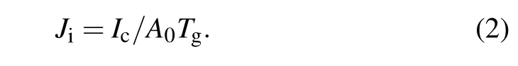
Because the growth of Ag films is closely related to the energy and flux density of ions impinging on the substrate, the ion energy and ion flux density were analyzed firstly.Figure 1 shows IVDF measured by RFEA.It can be found that at the power of 50 W,no obvious main peak can be seen, and only some small peaks are obtained.This indicates the random distribution of ion energy.As the power increased to 100 W,a main peak centered at the energy of 32.1 eV occurs except for other small peaks.This means that the interaction between VHF electric field and ions makes the most probable ion energy be about 32.1 eV.As the sputtering power further increases,the intensity of the main peaks increases,and the center position of peaks slightly shifts to higher energy.The full width at half maximum(FWHM)of these peaks also increases,from about 7.0 eV to 12.7 eV.Thus the ions impacting the substrate have more of a wide energy range.
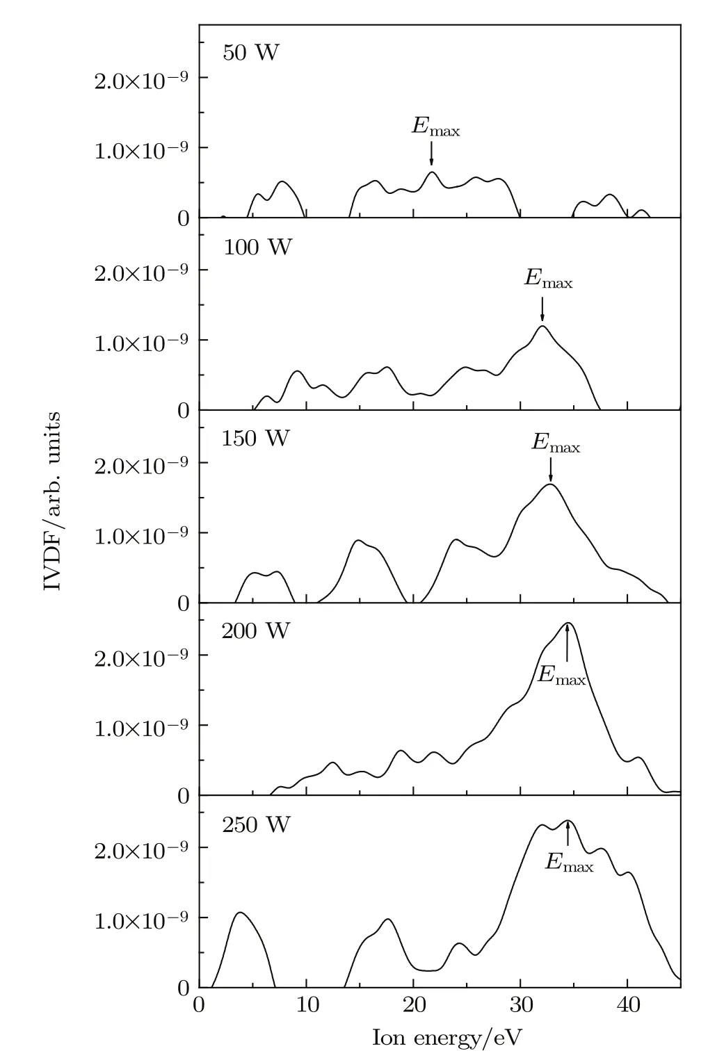
Fig.1.IVDFs of 60 MHz VHF magnetron sputtering at the sputtering power of 50–250 W.
Fig.2.Variation of maximum ion energy E max and ion flux density J i with the sputtering power.
Figure 2 shows the variation of maximum ion energy Emax(denoting the ion energy at the peak as shown in Fig.1) and ion flux density Jiwith the sputtering power.It can be seen that Emaxis about 21.8 eV at the power of 50 W,and then increases to the range of 32.1–34.5 eV as the power increased to 100–250 W.Jiincreases linearly from 0.0034 A/m2to 0.0145 A/m2.Because Emaxhas a small variation while Jiincreases rapidly as the power increases from 100 W to 250 W, the evolutions of initial growth behavior and microstructure feature of Ag films formation are mainly related to the ion flux.In additional,Emaxand Jiof 60 MHz magnetron sputtering are both lower than that of 13.56 MHz RF magnetron sputtering,which are in the range of 43.5—48.2 eV and 0.0057–0.0313 A/m2respectively at the sputtering power range of 50–250 W.Therefore,compared with the 13.56 MHz RF magnetron sputtering,the 60 MHz VHF magnetron sputtering can produce ions with lower energy and lower flux density.As a result,the growth of Ag films can be well controlled.
Figure 3 shows the SEM images of Ag films deposited at the sputtering power of 50–250 W.At the power of 50 W (Fig.3(a)),only some small bright dots in diameter of 10– 20 nm distribute randomly on the substrate surface,which correspond to Ag nanoparticles.Thus,at this stage,only low density Ag nanoparticles adsorp on the substrate surface,and no island growth takes place.At the power of 100 W(Fig.3(b)), the small bright dots in diameter of 10–20 nm and the big bright dots in diameter of 60–100 nm distribute simultaneously on the substrate surface.The small bright dots correspond to the Ag nanoparticles,while the big bright dots correspond to the Ag clusters,which are from the aggregation of small Ag nanoparticles.Thus,at this stage,the aggregation of small Ag nanoparticles and the formation of big Ag clusters take place.At the power of 150 W(Fig.3(c)),the Ag nanoparticles and Ag clusters form the nucleations simultaneously at the surface of the substrate.The size of major nucleations is about 6–23 nm,and the size of big nucleations coming from the few Ag clusters is about 90 nm.Thus,at this stage,the nucleation of Ag nanoparticles and Ag clusters take place simultaneously.At the power of 200 W(Fig.3(d)), the high density islands and low density coalescence of islands are seen.Thus,at this stage,the island growth dominates the films growth.At the power of 250 W(Fig.3(e)),only the worm-like microstructure[34]is formed while no islands can be found.The formation of the worm-like microstructure is from the more islands coalescence.Thus,at this stage,the island coalescence dominates the films growth.
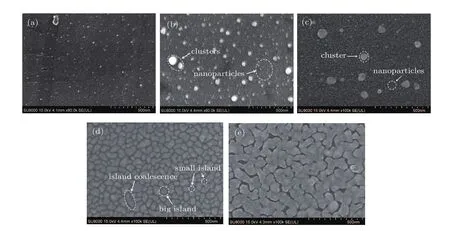
Fig.3.(color online)SEM images of Ag films deposited at 50–250 W by the 60 MHz VHF magnetron sputtering.
In addition,some evolutions of initial growth can be clearly observed in the samples prepared by the RF magnetron sputtering at the low power.Figure 4(a)shows the SEM image of Ag films deposited at 50 W by the 27.12 MHz sputtering. In this case,the growth surface is covered mainly by the high density islands,including the big islands and small islands, and the fewer island coalescence.The big islands are from the nucleations of clusters,while the small islands are from the nucleations of nanoparticles.Therefore,the development of nucleations from the clusters and nanoparticles simultaneously leads to the islands growth and the difference in the islands size.Figure 4(b)shows the SEM image of Ag films deposited at 50 W by the 13.56 MHz sputtering.It can be seen that the density of islands coalescence has increased largely compared with that of Fig.3(d),but the worm-like microstructure is not as complete as that of Fig.3(e).Meanwhile,some islands can still be seen.Therefore,the coalescence of islands is developed gradually from the low density to the high density.
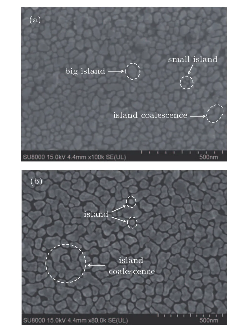
Fig.4.SEM images of Ag films deposited at 50 W by(a)27.12 MHz and(b)13.56 MHz magnetron sputtering.
For the initial stages of Ag film formation,according to the STM view of the initial stages of polycrystalline Ag film formation on an amorphous substrate,Polop makes a summary on the morphology evolution of the Ag films.[9]The initial stages of Ag films include the following stages:(i)the nucleation and island growth,(ii)the island coalescence,and (iii)the continuous film.However,no further information is reported in this summary on what happens before nucleation and after polycrystalline islands.From the above SEM observations in this work,it can be found that before the nucleation, the Ag nanoparticles firstly adsorp on the substrate,then forming Ag clusters by nanoparticles aggregation.After that,the Ag nanoparticles and clusters form the nucleations simultaneously for the islands formation,the islands coalescence,and the formation of Ag thin films.
Figure 5 shows the variation of particles density(nanoparticle, nucleation,or island)with the sputtering power.At the beginning of Ag films formation,the density of Ag nanoparticles on the substrate surface is very low,only about 1.4× 10¹⁴–1.9×10¹⁴m?2,far lower than that of nuclei(≈1× 10¹⁶m?2).[8]Thus,the nucleation of adsorped Ag nanoparticles cannot take place.With the increase of adsorped Ag nanoparticles,the aggregation of some Ag nanoparticles forms Ag clusters.The Ag nanoparticlesand the Ag clustersform the nucleations simultaneously,and the density of nuclei increases to about 2.1×10¹⁵m?2.With the development of nucleation and the formation of islands,the density of island decreases to about 2.6×10¹⁴m?2.Therefore,the variation of particles density(nanoparticle,nucleation,or island)indicates the evolution of the adsorption of Ag nanoparticles,the nucleations, the formation of islands,and the coalescence of islands.
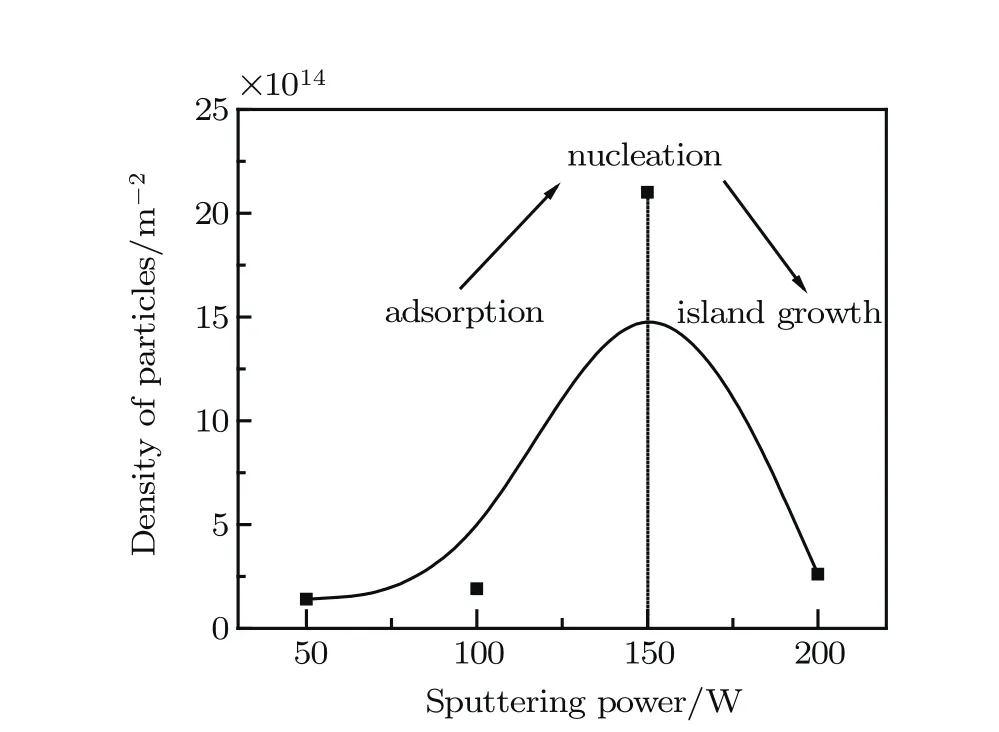
Fig.5.Variation of particles density(nanoparticle,nucleation,or island)with sputtering power.
Figure 6 shows the 3D AFM images of Ag films deposited at the sputtering power of 50–250 W.At the power of 50 W (Fig.6(a)),the adsorped Ag nanoparticles show some small lonely protrusions on the surface of the substrate.Atthe power of 100 W(Fig.6(b)),some big protrusions and high density small protrusions,corresponding to the Ag clusters and the Ag nanoparticles respectively,stand simultaneously on the surface of the substrate.At the power of 150 W(Fig.6(c)),the size of big protrusions increases,and the small protrusions of nucleations among the big protrusions can also be found.At the power of 200 W(Fig.6(d)),the islands all exhibit the shape of cone protrusions.At the power of 250 W(Fig.6(e)),the islands coalescence also exhibits the shape of cone protrusions, but the size of cone protrusions increases.
From the AFM measurement,the RMS roughness of samples were calculated.Figure 7 shows the variation of RMS roughness with the sputtering power.It can be found that at the stages of nanoparticles adsorption,the coverage of small density nanoparticles on the substrate surface leads to a low RMS roughness.With the formation of Ag clusters by nanoparticles aggregation and nucleations,the lonely particles standing on the surface of the substrate leads to a coarse surface,thus the large RMS roughness is obtained.When the formation of islands and the coalescence of islands take place,the number of boundaries between particles decreases.As a result,the surface of samples becomes smooth again.Thus,the RMS roughness decreases.
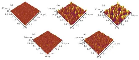
Fig.6.(color online)AFM images of Ag films deposited at 50–250 W by 60 MHz VHF magnetron sputtering.
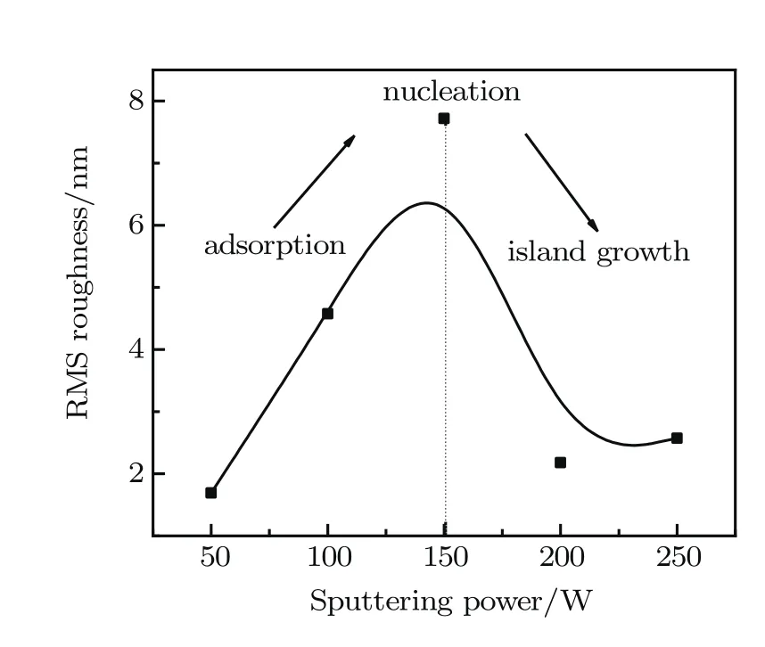
Fig.7.Variation of RMS roughness with sputtering power.
The x-ray diffraction of the Ag thin films grown on quartz crystal wafers were further measured for determining the structural phases of the initial stages of Ag films formation,as shown in Fig.8.Here,in order to avoid the hiding of weak Ag diffraction peaks by the strong Si diffraction peaks, the quartz crystal wafers while not the silicon wafer was used as the substrate.It can be seen that at the stages of Ag nanoparticles adsorped on the substrate,the formation of Ag clusters by small Ag nanoparticles aggregation,and the nucleation of Ag nanoparticles,no diffraction peak can be found.However, at the stages of the island growth,the small diffraction peak of Ag(111)can be seen,indicating the formation of crystal microstructures.When the coalescence islands form the worm like microstructure,the small diffraction peak of Ag(220)can also be seen except for the obvious Ag(111)diffraction peak. This means the formation of the polycrystalline structures with the preferred plane(111).Thus,the formation of Ag crystalline structures takes place at the stage of the island growth and coalescence.
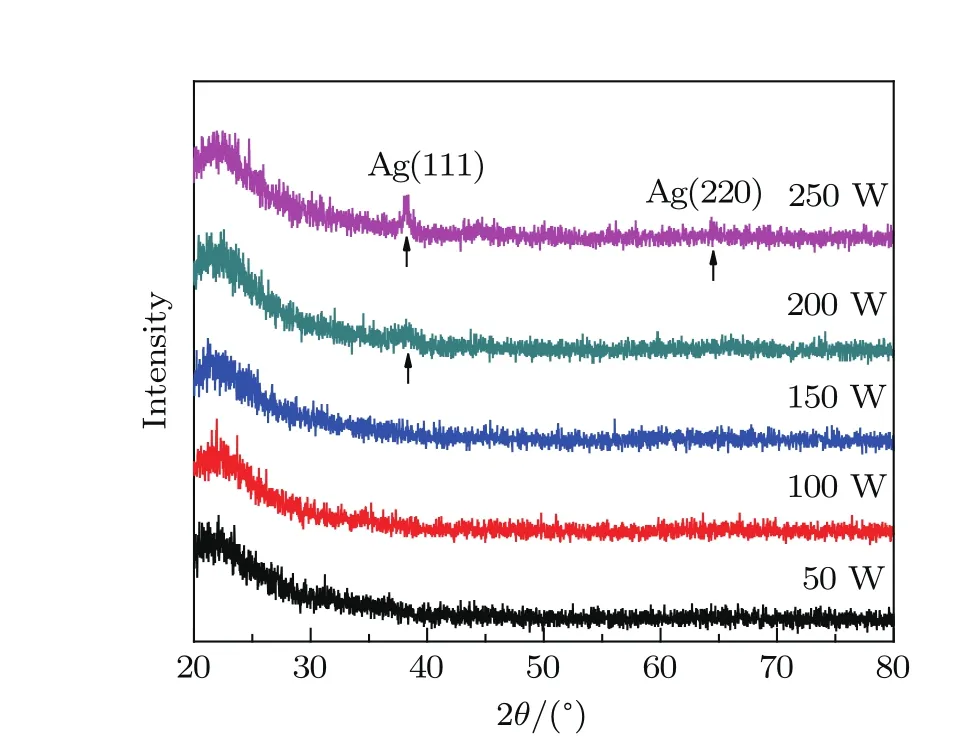
Fig.8.(color online)X-ray difractogram for the initial stages of Agfilms formation.
4.Conclusion
The initial formation stages are decisive for morphological and microstructure features of Ag films,but the investigations on the initial stages of Ag films formation are incomplete due to a lack of information on the nucleation stage.In this work,using 60 MHz magnetron sputtering,because of the moderate ions energy and lower flux density,the exact control of the initial growth of Ag films was achieved by varying the sputtering power from 50 W to 250 W.From the SEM observations,it can be found that before the nucleation,the Ag nanoparticles firstly adsorp on the substrate,then forming Ag clusters by nanoparticles aggregation.After that,the Ag nanoparticles and clusters form the nucleations simultaneously.These stages provide the nucleation for the islands formation,the islands coalescence,and the Ag thin films are formed.Therefore,the whole initial growth of Ag films follows the island thin-film growth modes(Volmer–Weber,VW), which are(i)the Ag nanoparticles adsorped on the substrate, (ii)the formation of Ag clusters by Ag nanoparticles aggregation,(iii)the nucleation by Ag nanoparticles and Ag clusters simultaneously,(iv)the islands formation,and(v)the coalescence of islands and the formation of polycrystalline Ag films.
[1]Guillén C and Herrero J 2015 Appl.Surf.Sci.324 245
[2]Nakanishi Y,Kato K,Omoto H and Yonekura M 2013 Thin Solid Films 532 141
[3]Kumar M,Jangid T,Panchal V,Kumar P and Pathak A 2016 Nanoscale Res.Lett.11 454
[4]Guillén C and Herrero J 2013 J.Phys.D-Appl.Phys.46 295302
[5]Sone J,Yamagami T,Aoki Y,Nakatsuji K and Hirayama H 2014 New J.Phys.16 095004
[6]Liu Z L,Wang M X,Xu J P,Ge J F,Le Lay G,Vogt P,Qian D,Gao C L,Liu C and Jia J F 2014 New J.Phys.16 075006
[7]Arafune R,Lin C L,Kawahara K,Tsukahara N,Minamitani E,Kim Y, Takagi N and Kawai M 2013 Surf.Sci.608 297
[8]Koch R 1994 J.Phys.-Condens.Mat.6 9519
[9]Polop C,Rosiepen C,Bleikamp S,Drese R,Mayer J,Dimyati A and Michely T 2007 New J.Phys.9 74
[10]Placidi E,Fanfoni M,Arciprete F,Patella F,Motta N and Balzarotti A 2000 Mater.Sci.Eng.B 69–70 243
[11]Bulí? J,Novotny M,Lan?ok J,Fekete L,Drahokoupil J and Musil J 2013 Surf.Coat.Technol.228 S86
[12]Zhu G and Wang T L 2015 Appl.Surf.Sci.324 831
[13]Bal J K and Hazra S 2009 Phys.Rev.B 79 155412
[14]Elofsson V,L?B,Magnf?lt D,Münger E P and Sarakinos K 2014 J. Appl.Phys.116 044302
[15]Guo J M,Ye C,Wang X Y,Yang P F and Zhang S 2017 Chin.Phys.B 26 065207
[16]Gu J H,Si J L,Wang J X,Feng Y Y,Gao X Y and Lu J X 2015 Chin. Phys.B 24 117703
[17]Jabbar S,Ahmad R and Chu P K 2017 Chin.Phys.B 26 010702
[18]Huang S H and Liu J 2014 Chin.Phys.B 23 058105
[19]Xiu X W and Zhao W J 2012 Chin.Phys.B 21 066802
[20]Zhao Y,Gao W,Xu B,Li Y A,Li H D,Gu G R and Yin H 2016 Chin. Phys.B 25 106801
[21]Kato K,Omoto H and Takamatsu A 2010 Vacuum 84 587
[22]Kato K,Omoto H and Takamatsu A 2012 Thin Solid Films 520 4139
[23]Kawamura M,Abe Y and Sasaki K 2006 Thin Solid Films 515 540
[24]Novotny M,Bulí? J,Pokorny P,Lan?ok J,Fekete L,MusilJ and ?ekada M 2013 Surf.Coat.Technol.228 S466
[25]Pongbordin U,Nurak G and Chaweewan S 2016 RSC Adv.6 7661
[26]He H J,Ye C,Wang X Y,Huang F P and Liu Y 2014 ECS J.Solid State Sci.Technol.3 Q74
[27]Gao M W,Ye C,Wang X Y,He Y S,Guo J M and Yang P F 2016 Chin. Phys.B 25 075202
[28]Huang F P,Ye C,He H J,Liu Y,Wang X Y and Ning Z Y 2014 Plasma Sources Sci.Technol.23 015003
[29]Ye C,He H J,Huang F P,Liu Y and Wang X Y 2014 Phys.Plasma 21 043509
[30]Ellmer K,Wendt R and Wiesemann K 2003 Int.J.Mass Spectrom. 223–224 679
[31]Seeger S,Harbauer K and Ellmer K 2009 J.Appl.Phys.105 053305
[32]Stranak V,Drache S,Bogdanowicz R,Wulff H,Herrendorf A,Hubicka Z,Cada M,Tichy M and Hippler R 2012 Surf.Coat.Technol.206 2801
[33]Stranak V,Wulff H,Bogdanowicz R,Drache S,Hubicka Z,Cada M, Tichy M and Hippler R 2011 Eur.Phys.J.D 64 427
[34]Palanisamy S,Yan L Q and Zhang X H 2015 Anal.Methods 7 3438
19 May 2017;revised manuscript
12 June 2017;published online 31 July 2017)
10.1088/1674-1056/26/9/095206
?Project supported by the National Natural Science Foundation of China(Grant Nos.11675118 and 11275136).
?Corresponding author.E-mail:cye@suda.edu.cn
?2017 Chinese Physical Society and IOP Publishing Ltd http://iopscience.iop.org/cpb http://cpb.iphy.ac.cn

- Chinese Physics B的其它文章
- Relationship measurement between ac-Stark shift of 40Ca+clock transition and laser polarization direction?
- Air breakdown induced by the microwave with two mutually orthogonal and heterophase electric field components?
- Collective motion of active particles in environmental noise?
- Temperature dependence of heat conduction coefficient in nanotube/nanowire networks?
- Analysis of dynamic features in intersecting pedestrian flows?
- Heat transfer enhancement in MOSFET mounted on different FR4 substrates by thermal transient measurement?