Design and analysis on four stage SiGe HBT low noise amplifier①
2015-04-17 06:27:11JingkaiZhuangYiqiLiZhenrong
High Technology Letters 2015年3期
Jing kai (井 凱), Zhuang Yiqi, Li Zhenrong
(*Department of Microelectronics, Xidian University, Xi’an 710071, P.R.China)(**State Key Laboratory of Wide Band Gap Semiconductor, Xi’an 710071, P.R.China)
?
Design and analysis on four stage SiGe HBT low noise amplifier①
Jing kai (井 凱)*, Zhuang Yiqi*, Li Zhenrong②
(*Department of Microelectronics, Xidian University, Xi’an 710071, P.R.China)(**State Key Laboratory of Wide Band Gap Semiconductor, Xi’an 710071, P.R.China)
Focusing on the linearity shortcoming on a bipolar low noise amplifier (LNA), a new 6~14GHz four stage SiGe HBT LNA is proposed. This amplifier adopts a method of gain allocation on multiple stages to avoid the limitation on linearity especially with the addition of negative gain on the third stage. To realize gain flatness, extra zero is introduced to compensate the gain roll-off formed by pole, and local shunt-shunt negative feedback is used to widen the bandwidth as well as optimize circuit’s noise. Simulated results have shown that in 6~14GHz, this circuit achieves noise figure (NF) less than 3dB, gain of 17.8dB (+0.2dB), input and output reflection parameters of less than -10dB, and the K factor is above 1.15.
low noise amplifier (LNA), pole-zero cancellation, noise figure (NF), SiGe HBT BJT, linearity
0 Introduction
In recent years, wireless communication has been thrived in the fields of commercial and scientific research. For example, 2.4 GHz ISM band consists of many communication protocols, such as WLAN IEEE 802.11 b/g, Bluetooth and IEEE 802.15.4[1-3]. Along with the growing up of 3G technology in mainland, faster and more power efficient wireless communication systems have emerged in the electronic market. Since the U.S. Federal Communications Commission (FCC) approved the application of ultra-wideband (UWB) technology for commercial use in early 2002, ranging from 3.1 to 10.6GHz[4], more and more UWB transceivers have been implemented. It is believed that higher frequency band will be utilized before long.
Because of the high power consumption in RF systems, bipolar transistors have higher transconductance than MOS devices and they are good to be implemented in RF circuits[5]. However, with the linear limitation on I-V exponential characteristic, bipolar devices can hardly implement a very good linear performance which is more evident in single-stage amplifier[6]. Non-linearity arises from the sum of deviations on the quiescent operating point of all devices as the input-signal amplitude increases, such as 1dB compression. The worst effect of non-linearity is that surrounding interferes around the signal frequency will cause intermodulation
and cross-modulation which are in fact should be minimized. There are a few ways to alleviate the non-linear problem, and one efficient way is to use the Volterra Series to modify the quiescent operating point and components. This is, however, definitely at the cost of optimized gain and noise performance. In order to address this problem, changing structure is a more thorough method: multi-stage amplifying can avoid one-stage over amplifying, thus avoiding non-linearity, and because there are many stages, multiple feedbacks can be added into performance optimization, increasing the flexibility of circuit designing.
Focusing on the application prospect of UWB band and higher frequency band and the fact of linear shortcoming in bipolar devices, a new multi-stage low noise amplifier (LNA) is proposed. This LNA adopts a gain allocation scheme to avoid the gain overshoot in one stage which causes non-linearity. Shunt-shunt feedback is utilized in the input terminal to make good S11guaranteed. The third stage introduces an extra zero to compensate the roll-off caused by pole. Local negative feedback is used to low down the noise and widen the bandwidth. Results have shown that this design method is useful in designing RF LNA and integrated MMIC.
1 Structure of proposed LNA
The schematic of proposed LNA is shown in Fig.1 below. C2, C4, C5, C6and C7are DC decouple capacitors, transistors Q1, Q2, Q3and Q4are amplifying stages of LNA, Q5is the output buffer stage. Because the gain of the fifth stage is about 1, merely acting as an output match cell whose amplifying function is not taken into account. R1, R2, R3, R4, R10are the corresponding loads of these four amplifying stages. R5, R6, R7, R8are feedback resistors. C8and R9are used to broaden gain bandwidth. C1is the equivalent capacitance of pad; inductor L1is used for input match, L2is utilized to produce an extra zero. R11and R12are adopted for output match. In Fig. 1, Zin1and Zin2are the input impedance looking into the first stage and second stage.
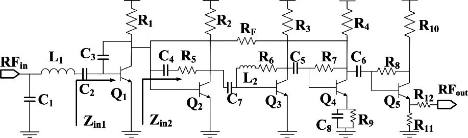
Fig.1 Schematic of four-stage SiGe HBT LNA
1.1 LNA input match
The input match scheme can be discussed from the RLC series network, which is shown in Fig.2.
(1)
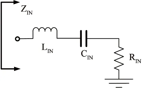
Fig.2 Schematic of second-order RLC series match network
And input reflection parameter can be derived as
(2)
In Eq.(2), RSis the source resistance of input port, that is, 50 Ω. In order to maintain a small input reflection, S11should meet
20log|S11|≤-10dB
(3)
Combining Eqs(2) and (3) and after some math derivations, the input match bandwidth Δf is
(4)
Δω10dBis Δf multiplied by 2π. From Eq.(4) the match bandwidth is in inverse proportion to LIN. The larger LINis, the narrower bandwidth can achieve. This relationship can be understood in the LC network’s Q factor in another way[5]. As the inductor’s value arises, the impedance peak value of LC network goes up higher with the shrinking of bandwidth. So when the series RLC has a small LIN, the input network is actually a low Q factor series network with a corresponding large bandwidth. Referring to Eq.(4), operation bandwidth is 8GHz, so the maximum inductor value is 0.66nH. In the real design, however, parasitic parameters will deteriorate the post-simulated results; it is usually practicable to introduce a smaller inductor to compensate this band-narrowing effect.
After determining LIN, series capacitor CINneeds to be quantified. The center frequency ω0in series network is shown below in Eq.(5). From Eq.(5), there exists a compromise between LINand gain: As the operating band and center frequency are determined, larger capacitor needs a smaller inductor to hold the center frequency unchanged, and Base-Emitter capacitor is proportion to the transconductance of bipolar[7], that means in order to have a larger gain on the first stage of LNA, smaller inductor should be used. Optimization can be done to increase the first amplifying stage’s gain by shrinking the inductor so that wider bandwidth and lower NF can be achieved. In this LNA, inductor LINof 0.38 nH and capacitor CINof 190 fF are chosen.
(5)
Capacitor CINcan be formed by shunt-shunt feedback topology[8-10]. Shunt-shunt feedback can achieve a wider bandwidth and good noise performance as the first amplifying stage. From Fig.1 and Fig.2, the series parameters RINand CINcan be expressed as
CIN=CBE,Q1+(C3+CBC,Q1)(1+GM1ZL1)
(6)
(7)
CBE,Q1is the base-emitter capacitor of Q1, CBC,Q1is the base-collector capacitor, GM1is the effective transconductance of Q1, ZL1is the impedance looking from the collector of Q1. After determining the gain and GM1of Q1, other parameters can be confirmed.
1.2 LNA gain allocation technique
It is known that linearity and gain have a compromise relationship
(8)
IIP3i(i=1,2,…n) and Gai(i=1,2,…n) are the third-order intercept point and available power gain in every subsystem, and each amplifying stage in LNA can be directly treated as a subsystem. With Eq.(8), gain allocation can be altered to achieve a good linear characteristic, it can be derived as
IIP3(dBm)≈IIP3n-1,n(dBm)-G1·G2·…… ·Gn(dB)+Gn(dB)
(9)
IIP3n-1,nis the last stage’s linearity, Giis the gain on each stage. Considering the bipolar nonlinear characteristic[7]and Fig.1, Eq.(9) can be altered as
(10)
G is the total gain of LNA, G4is the fourth stage gain, and resistors are shown in Fig.1. From Eq.(10), if more gain can be allocated in the last stage, better linearity can be achieved.
Large gain on the first stage of LNA can help it to reduce noise[11], so with total gain determined, more gain should be given to the first and the last stage, not the middle stages. Traditional LNAs allocate gain in every stage[2-4,8, 9], which is not good for noise and linearity because some gain is wasted in the middle stages. In this paper, negative gain (<0dB) is chosen on the third stage, so noise can be further lowered and linearity can be enhanced. The total gain is first set to 20 dB, so 26dB, 2dB, -12dB and 4dB are allocated on these four stages. With Eq.(10), IIP3 is -13.2dBm.
1.3 Pole-zero cancelling and gain flattening
For wideband LNA, especially when adopting the OFDM modulation scheme, gain flatness is required[12]. Multiple gains can introduce many poles easily which can draw down the power gain. Fig.3 shows corresponding gain curve along with frequency of the four stages, and RC parallel tank in the fourth stage is omitted for simplicity. Fig.4 shows the small-signal equivalent circuit of proposed LNA. Illustrations on this zero-cancelling technique are discussed below.
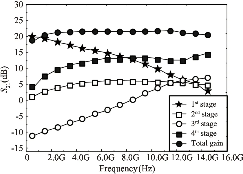
Fig.3 Gain curve of four stages with frequency
Fig.4 neglects the large resistance feedback resistors and because R6is small which should be taken into calculation. DC decouple capacitors are omitted as their impedances are small in the discussion band. GM,Qi(i=1,2,3,4) is the effective transconductance of every stage, Cπ,Qiis the capacitor looking into base. Because the last stage’s gain is near to 1, only its base capacitance is added into pole computing. When input match satisfies, the signal voltage drop on Q1’s base is
(11)
VSis the voltage source, there are two nets in first stage, base net and collector net, and they may introduce two poles. Section 1.1 has shown that base capacitor should be added into input series match network, so base net will not introduce pole. This effect seems awkward, but can be explained: RC time constant method holds in the loop with resistors and capacitors, base capacitor in Q1connects inductor which does not satisfy the method which should be directly treated in this manner.
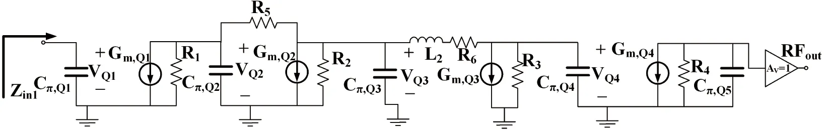
Fig.4 LNA small signal equivalent circuit
Poles’ location should be determined first, especially the main pole in LNA. With the knowledge of Gain-Bandwidth Product[7], large gain will lead to a low pole, namely, bandwidth. Referring to gain allocation in Section 1.2, it can be derived that the main pole should be located at first stage; this can be verified in Fig.3 where gain roll-off exists on the first stage curve. In the other stages, there are no evident voltage drops. This is due to the good performance of SiGe HBT device whose cutting-off frequency can easily achieve nearly 200GHz. Zero can be created to cancel out the main pole of LNA, which can be illustrated in small-signal equations
(12)
(13)

(14)
(15)
(16)
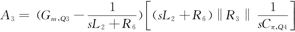
Ai(i=1-4) are the small-signal gains of the fourth stage, from Eqs(13)~(16), each RC load introduces a pole, 1/RC. From Fig.3, the first stage shows a gain roll-off in 0~16GHz, whereas the second and fourth stages are not. The third stage’s structure is different from others which should be analyzed. Because its gain is smaller than the second and fourth stages, and the load’s pole frequency is rather higher than these poles, Eq.(15) can be simplified as
A3=Gm,Q3[(sL2+R6)‖R3]
(17)
Transconductance in Eq.(17) is simplified as well based on the assumption that the intrinsic gain Gm,Q3R6is larger than 1. So the corresponding zero is
(18)
Poles and this zero are all located in the frequency Left Half Plane so zero can cancel out the main pole, avoiding gain roll-off. From Fig.3, it is shown that the total gain is flat across the discussion band. Attention should be paid that the third stage’s gain is below 0dB in the lower band. This gain curve can be explained as follows: In the lower band, the impedance of feedback inductor is small, and with small value of R6, the third stage actually acts as a diode connection, rather than an amplifying condition. As the frequency goes up, isolation between base and collector increases with the increase of impedance of inductor. The gain in this stage will go up as frequency increases. This is in agreement with zero function.
With the pole-zero cancelling technique, gain flatness can be optimized in a further way. This paper adopts two more optimization techniques, local negative feedback and RC tank structure (located in fourth stage). Noise cancelling technique can be utilized to low down the noise from the output terminal of the first stage[13-15], and feedback can be used to broaden bandwidth, which is done by pushing all the poles in the feedback loop to a higher frequency, attenuating the gain impact of the last three poles. In the fourth stage, parallel RC tank is used to adjust the little drop at high frequency caused by some undesired parasitic influences[16]. These three techniques can achieve a very good gain flatness, where simulated results show a 17.8dB S21with the variation of only 0.4dB.
2 LNA parameters and layout
This proposed wide band LNA is designed and post-simulated in a Jazz 0.18μm SiGe HBT technology. Table 1 shows the parameters in Fig.1, DC decoupling capacitors are all 1 pF and are not listed. Layout is shown in Fig.5 with pads and the die area is 0.553mm2(0. 537mm×1.03mm), this LNA uses two inductors and its area is comparable to state-of-art SiGe HBT LNA[17](0.515 mm2). However, this LNA has a better performance (bandwidth and linearity).
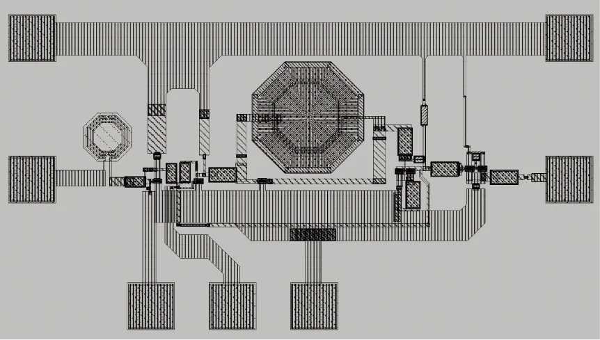
Fig.5 Layout of proposed SiGe HBT LNA
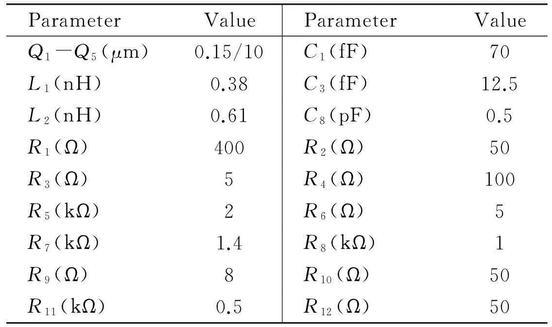
ParameterValueParameterValueQ1-Q5(μm)0.15/10C1(fF)70L1(nH)0.38C3(fF)12.5L2(nH)0.61C8(pF)0.5R1(Ω)400R2(Ω)50R3(Ω)5R4(Ω)100R5(kΩ)2R6(Ω)5R7(kΩ)1.4R8(kΩ)1R9(Ω)8R10(Ω)50R11(kΩ)0.5R12(Ω)50
3 Results and discussion
The wide band LNA is designed by Jazz 0.18μm SiGe HBT technology and post-simulated by Cadence Spectre tool to analyze the chip layout.
Fig.6 shows the gain, input and output reflection parameters curves along with frequency. It is shown that in the band of 6~14 GHz, S11and S22are all less than -10dB, ensuring a good signal transmission. S21is 17.6dB~18dB, with a variation of merely 0.4dB. Because there is a quasi-diode connection at the third stage, the output signal can be easily injected into the input terminal of Q3, oscillation may occur to deteriorate the circuit’s stability. S11and S22are not sufficient to hold this condition. To ensure this, stability factor K is required to testify the oscillation problem[18], if K is larger than 1, the system is unconditional stable. Fig.7 is the K factor varying with frequency, which shows easily that even the value of K is not very large in the discussion band, it is still larger than 1, this LNA can keep stability unconditionally. As the frequency goes up, isolation in Q3is better and less chance of oscillation may occur. This is comparable to the curve of Fig.7; K goes up in the high frequency. Fig.8 is the NF vs. frequency. NF is less than 3.0dB across the band.
Fig.9 shows the IIP3at 11GHz. The intercepting point is -14.2dBm. This is in agreement with results of Section 1.2, which indicates that linearity can be quantified and enhanced with gain allocation scheme.
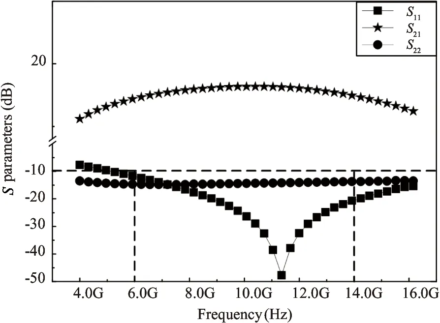
Fig.6 Simulation results: S11, S21 and S22
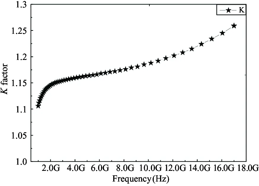
Fig.7 Simulation results of K factor
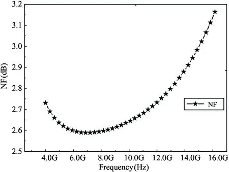
Fig.8 Simulation results of NF
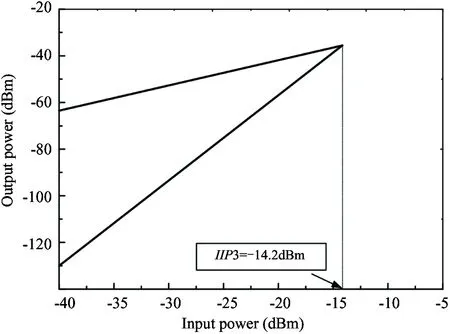
Fig.9 Simulation results of IIP3 at 11GHz
4 Conclusion
This paper presents a method of gain allocation scheme to address the nonlinearity of bipolar low noise amplifier. Compared to single-stage structure, this four-stage amplifier quantifies IIP3 and pole-zero cancelling technique is used to broaden the bandwidth to avoid the gain roll-off problem. This circuit achieves 8 GHz bandwidth and 17.8dB gain with the variation of 0.4dB. The die area with pads is 0.515mm2. Results have shown that gain flatness can be maximally achieved and noise is minimized to a very low value. It is estimated that this wide band LNA design can be useful for further research and application.
[ 1] Moreira C P, Kerherve E, Jarry P, et al. Design and implementation of a dual-band concurrent fully-integrated LNA for WLAN IEEE 802.11a/b/g Applications. International Journal of RF and Microwave Computer-Aided Engineering, 2009, 19(1): 1-13
[ 2] Zhang L J, Li L N. Research on optimizing the noise figure of low noise amplifier method via bias and frequency. The Journal of China Universities of Posts and Telecommunications, 2011, 18(4): 118-122
[ 3] Maeda T, Yano H, Hori S, et al. Low-power-consumption direct-conversion CMOS transceiver for multi-standard 5GHz wireless LAN systems with channel bandwidths of 5-20 MHz. IEEE Journal of Solid-State Circuits, 2006, 41(2): 375-383
[ 4] Lin Y T, Chen H C, Wang T, et al. 3-10-GHz ultra-wideband low-noise amplifier utilizing miller effect and inductive shunt-shunt feedback technique. Microwave Theory and Techniques, IEEE Transactions on, 2007, 55(9): 1832-1843
[ 5] Razavi B, Behzad R. RF Microelectronics. New Jersey: Prentice Hall, 1998. 12-29
[ 6] Aparin V, Zeisel E, Gazzerro P. Highly linear SiGe BiCMOS LNA and mixer for cellular CDMA/AMPS applications. 2002 Radio Frequency Integrated Circuits (RFIC) Symposium, IEEE. 2002. 129-132
[ 7] Gray P R, Hurst P J, Meyer R G, et al. Analysis and Design of Analog Integrated Circuits. John Wiley & Sons, 2008. 3-9
[ 8] Shen P, Zhang W R, Jin D Y. Design and analysis of an ultra-wideband SiGe HBT low noise amplifier. Chinese High Technology Letters, 2011, 21(001): 77-82 (In Chinese)
[ 9] Zhang H, Fan X, Sinencio E S. A low-power, linearized, ultra-wideband LNA design technique. IEEE Journal of Solid-State Circuits, 2009, 44(2): 320-330
[10] Ding C B, Zhang W R, Jin D Y, et al. Design of SiGe HBT UWB low noise amplifier based on darlington cascode structure. Chinese High Technology Letters, 2012, 22(10): 1070-1076 (In Chinese)
[11] Weststrate M, Sinha S. Noise optimization of a wideband capacitive shunt-shunt feedback LNA design suitable for software-defined radio. In: Proceedings of the 16th IEEE International Conference on Electronics, Circuits, and Systems, Yasmine Hammamet, 2009. 619-622
[12] Zargari M, Terrovitis M, Jen S H M, et al. A single-chip dual-band tri-mode CMOS transceiver for IEEE 802.11 a/b/g wireless LAN. IEEE Journal of Solid-State Circuits, 2004, 39(12): 2239-2249
[13] Chen W H, Liu G, Zdravko B, et al. A highly linear broadband CMOS LNA employing noise and distortion cancellation. IEEE Journal of Solid-State Circuits, 2008, 43(5): 1164-1176
[14] Liao C F, Liu S I. A broadband noise-canceling CMOS LNA for 3.1-10.6-GHz UWB receivers. IEEE Journal of Solid-State Circuits, 2007, 42(2): 329-339
[15] Bruccoleri F, Klumperink E A M, Nauta B. Wide-band CMOS low-noise amplifier exploiting thermal noise canceling. IEEE Journal of Solid-State Circuits, 2004, 39(2): 275-282
[16] Eo Y S, Yu H J, Song S S, et al. A fully integrated 2.4 GHz low IF CMOS transceiver for 802.15. 4 ZigBee applications. In: Proceedings of the IEEE Asian Solid-State Circuits Conference, Jeju, Korea, 2007. 164-167
[17] Yang M, Ha M, Park Y, et al. A 3-10 GHz CMOS low-noise amplifier using wire bond inductors. Microwave And Optical Technology Letters, 2009, 51(2): 414-416
[18] Ruey L W, Min C L, Chih C L, et al. A 1V full-band cascade UWB LNA with resistive feedback. In: Proceedings of the 2007 IEEE Radio Frequency Integrated Technology, New York, USA, 2007. 188-190
Jing Kai, was born in 1987. He received the B.E degree in Microelectronics Department from Xi’Dian University. With satisfying performance in degree and scientific research, he is permitted to pursue the Ph.D directly and now a Ph.D candidate of a five-year educational system. He is a member at Department of RF Microwave Design System at Xi’Dian University, PRC. His research interests include the design of microwave circuits, noise research in LNA.
10.3772/j.issn.1006-6748.2015.03.017
①Supported by the National Natural Science Foundation of China (No. 61076101, 61204092, 61306033).
②To whom correspondence should be addressed. E-mail: allen_lzr@126.com Received on Mar. 15, 2014*, Lin Zhiyu***
 High Technology Letters2015年3期
- High Technology Letters的其它文章
- Improving the BER performance of turbo codes with short frame size based on union bound①
- Probabilistic data association algorithm based on ensemble Kalman filter with observation iterated update①
- A matting method based on color distance and differential distance①
- Probability density analysis of SINR in massive MIMO systems with matched filter beamformer①
- Edge detection of magnetic tile cracks based on wavelet①
- Diversity-multiplexing tradeoff of half-duplex multi-input multi-output two-way relay channel with decode-and-forward protocol①