發光層位置對白光有機發光二極管的影響
2015-04-05 09:02:02向東旭李海蓉謝龍珍楊佳明員朝鑫孫永哲
發光學報 2015年7期
關鍵詞:實驗室
向東旭, 李海蓉,2,3*, 謝龍珍, 楊佳明, 王 芳, 員朝鑫, 孫永哲
(1. 蘭州大學物理科學與技術學院 微電子研究所, 甘肅 蘭州 730000;2. 蘭州大學 磁學與磁性材料教育部重點實驗室, 甘肅 蘭州 730000;3. 特殊功能材料與結構設計教育部重點實驗室, 上海 200050)
發光層位置對白光有機發光二極管的影響
向東旭1, 李海蓉1,2,3*, 謝龍珍1, 楊佳明1, 王 芳1, 員朝鑫1, 孫永哲1
(1. 蘭州大學物理科學與技術學院 微電子研究所, 甘肅 蘭州 730000;2. 蘭州大學 磁學與磁性材料教育部重點實驗室, 甘肅 蘭州 730000;3. 特殊功能材料與結構設計教育部重點實驗室, 上海 200050)
同一種主體材料MADN中混摻不同的摻雜劑,分別制備了兩種白光有機發光二極管,測試并研究了它們的發光效率、壽命、發光亮度、電致發光光譜以及色平衡度。結果表明,兩種白光器件的性能受發光層的順序和厚度的影響顯著。發光層順序由陽極到陰極方向為橙/藍的器件的穩定性要優于發光層順序為藍/橙的器件,這是由于橙光發光層中的rubrene對空穴的陷進作用可捕獲穿越橙光發光層中的空穴,從而有效地調控了器件內部的電子、空穴濃度的平衡。通過對器件的優化,制得了色坐標為(0.320 1, 0.345 9)的接近標準白光的有機電致發光器件。
有機電致發光; 發光層順序與厚度; 載流子注入; 載流子平衡
1 Introduction
Organic light-emitting diodes (OLEDs) have attracted considerable interest due to their potential application in flat-panel displays and thin-film lighting devices[1-4]. Recently, impressive scientific and technological progress have been achieved in this field since Tang and V. Slyke reported their first low operation voltage driven OLED in 1987[5-9]. Blue OLED (BOLED) is a vital component for full-color display as well as solid-state lighting. Blue emitter is used as one of the three primary color sources or as the color converter light source to obtain green or red emission from the fluorescent materials[10-14]. However, a number of technological challenges still need to be resolved for BOLED,e.g., increasing device efficiency, lowering driving voltage, and improving the operational stability.
Continual efforts have been made towards exploring blue-emitting materials and device structures to improve the performance of OLEDs. In a variety of methods, doping is an effective way to improve the efficiency of OLEDs[15-18]. In this paper, we studied the device structure, especially the fluorescent materials doped light-emitting layer (EML). The fluorescent dye 4, 4-bis[4-(di-ptolylamino)styryl] biphenyl (DPAVBi) has been commonly used as blue fluorescent dopant and several works have been done to improve the efficiency of the DPAVBi based BOLEDs. Here we presented the BOLED with the EML in which DPAVBi was doped in the host 2-methyl-9,10-di(2-naphthyl)-anthracene (MADN). Variation of the thickness of EML affects not only the electrical characteristics of the devices but also the optical properties. And the blue device with a 15-nm-thick EML shows higher current efficiency than that reported in Ref.[19].
White-light emission originating from the blend of two complementary colors has been widely researched. The fluorescent dye 5,6,11,12-tetraphenylnaphthacene, rubrene (denoted Rb), has been primarily used as an orange dopant in OLEDs. It has been proved that an excellent orange emission can be obtained by doping Rb in either n-type or p-type host. In order to fabricate white OLED (WOLED), we added an orange EML by doping Rb in MADN in BOLED. The effects of the stack order of EMLs on WOLEDs performance were investigated. It was found that the WOLED with an EML sequence of orange/blue showed better stability than that with an EML sequence of blue/orange. In addition, we optimized the performance of the WOLED with an EML sequence of orange/blue.
2 Experiments
As a hole injection material, 4, 4′, 4″-tris[phenyl(3-methylphenyl)amino]triphenylamine (m-MTDATA) film was thermally deposited on top of indium tin oxide (ITO) substrate. Then, N,N-diphenyl-N,N-bis(1-naphthyl)-(1,1-biphenyl)-4,4-diamine (α-NPB) film (as hole transport layer, HTL) was deposited on m-MTDATA film and subsequently the EML was deposited onα-NPB film. Next, 2,9-dimethyl-4,7-diphenyl-1,10-phenanthroline (BCP) film (as hole blocking layer) was deposited on the EML. Following that, tris(8-hydroxy quinoline)-aluminium (Alq3) film (as electron transport layer) was deposited on BCP film. Finally, Al cathode electrode was deposited on Alq3film. The device with the configuration of ITO/m-MTDATA/NPB/MADN∶DPAVBi(6%, mass fraction) (xnm)/BCP/Alq3/Al was denoted as device A, the devices with the structure of ITO/m-MTDATA/NPB/MADN∶rubrene(1%, mass fraction)(5, 10,15 nm)/ MADN∶DPAVBi(6%, mass fraction) /BCP /Alq3/Al were denoted as device B, D, and E, respectively. And the device with the structure of ITO/m-MTDATA/NPB/MADN∶DPAVBi(6%, mass fraction)/MADN∶Rubrene(1%, mass fraction)/BCP/Alq3/Al was denoted as device C, as shown in Fig.1, the thickness of all devices shown in Table 1. All the organic materials in this study were purchased from Aldrich Chemical Co., Ltd., and their purity is more than 99%. The chamber pressure during deposition was kept at 4×10⁻⁴Pa and the deposition rate was 0.2-0.3 nm/s. The film thickness was monitored by a quartz crystal oscillator. The device active area was 3.5 mm× 3.5 mm. All the devices were encapsulated by epoxy resin in N2atmosphere. The current density-voltage and the luminescence characteristics were measured by a Minolta LS-110 luminance meter with a Kiethley 2410 programmable current-voltage digital source unit. The electroluminescence (EL) intensities of devices and the CIE coordinates were measured by Photo Research PR-650 after encapsulation. All the measurements were performed in air at room temperature.
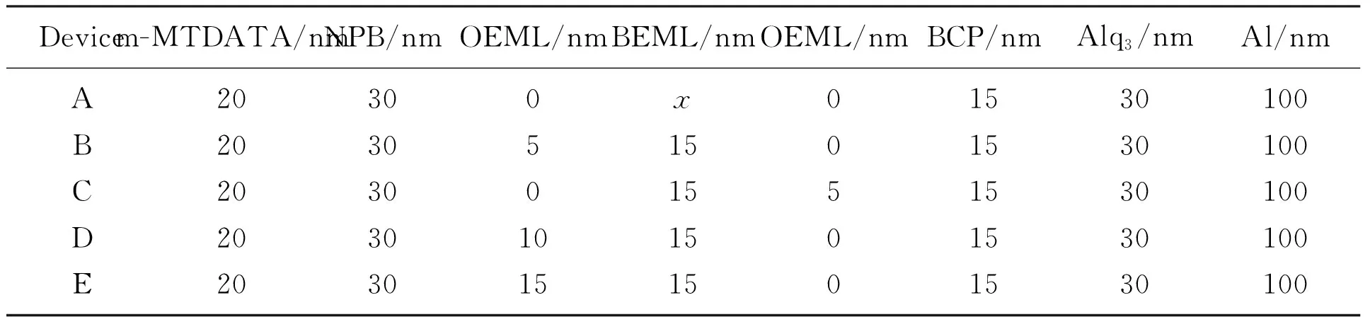
Table 1 Device structure in the article
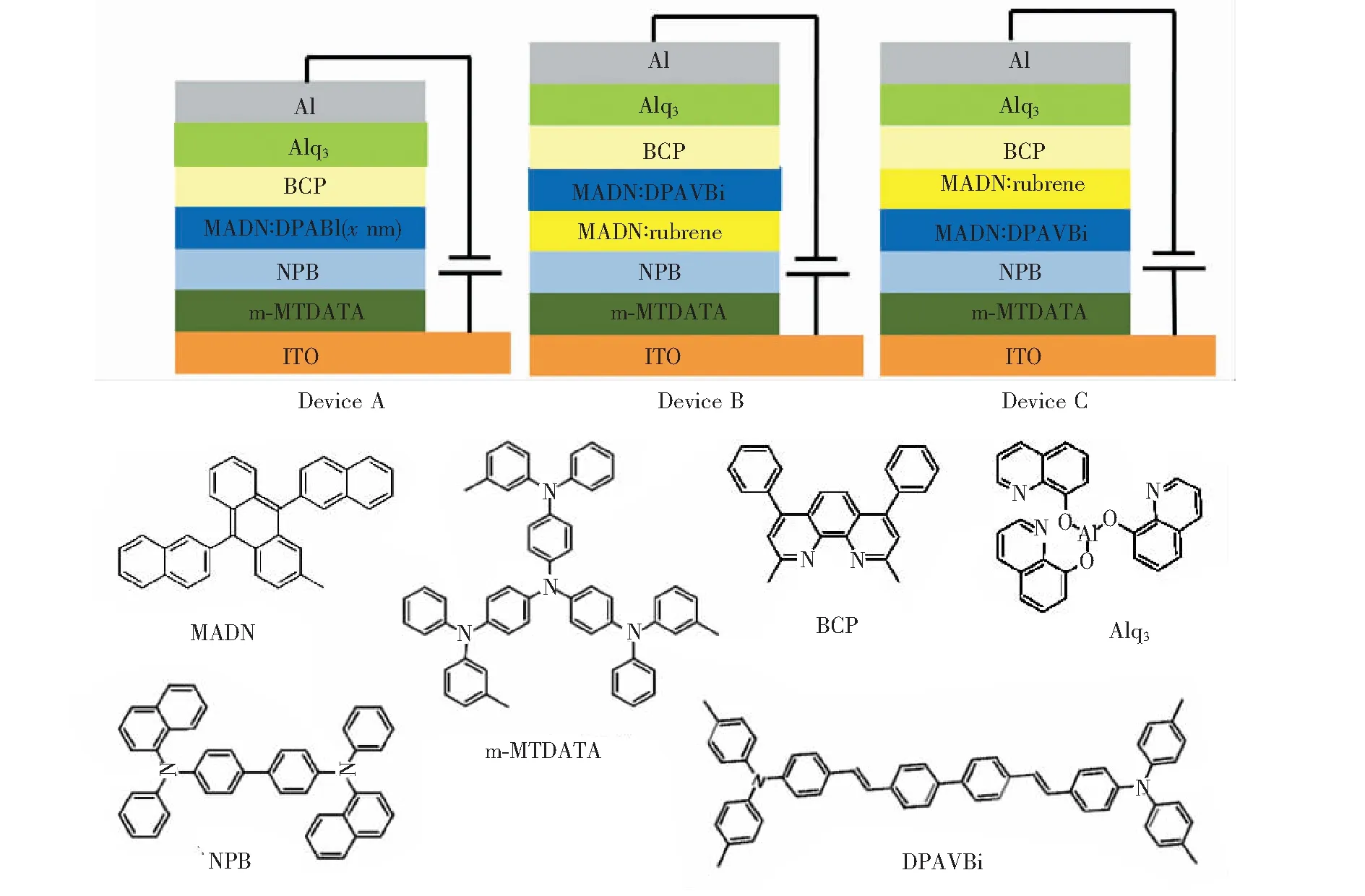
Fig.1 Devices structure and molecular formula of organic materials used in this study
3 Results and Discussion
Fig.2(a) shows EL spectra of device Avs. EML thickness, which were measured at a brightness of~10 000 cd·m-2. It is clear that the peaks of the EL spectra of the BOLEDs are at about 466, 495,530 nm, respectively, which are attributed to the electronic vibration transition from excited state (S1) to the ground state (S0) in DPAVBi. The three peaks (466, 495,530 nm) are attributed to 0s1-0s0, 0s1-1s0and 0s1-2s0transition[20], respectively, as shown in the inset of Fig.2(a). It is found that the EL spectra of device A changes varying with the EML thickness. According to related reports[21], the 0-0 vibrational component at 466 nm is much stronger than any other vibrational component. Interestingly, the intensity of the 0-1 component at 495 nm increases with the increasing of EML thickness. The change of the EL spectra may be due to a planar optical microcavity effect, which increases the intensity of the shoulder peak at 495 nm in the line-spectral shape through the light reflection and interference depending on the EML thickness in the multi-layer structure (Fig.4(a))[19,22]. Multiple beam interference between parallel reflectors leads to a spectral emission intensity enhancement[23]. The CIE coordinates of device A with the EML thickness of 15, 20, 25, 30 nm are (0.164 6, 0.228 6), (0.169 7, 0.233 0), (0.178 6, 0.283 3), and (0.200 9, 0.316 3), respectively. The color varies from blue to blue-green with EML thickness increasing, as shown in Fig.2(b).
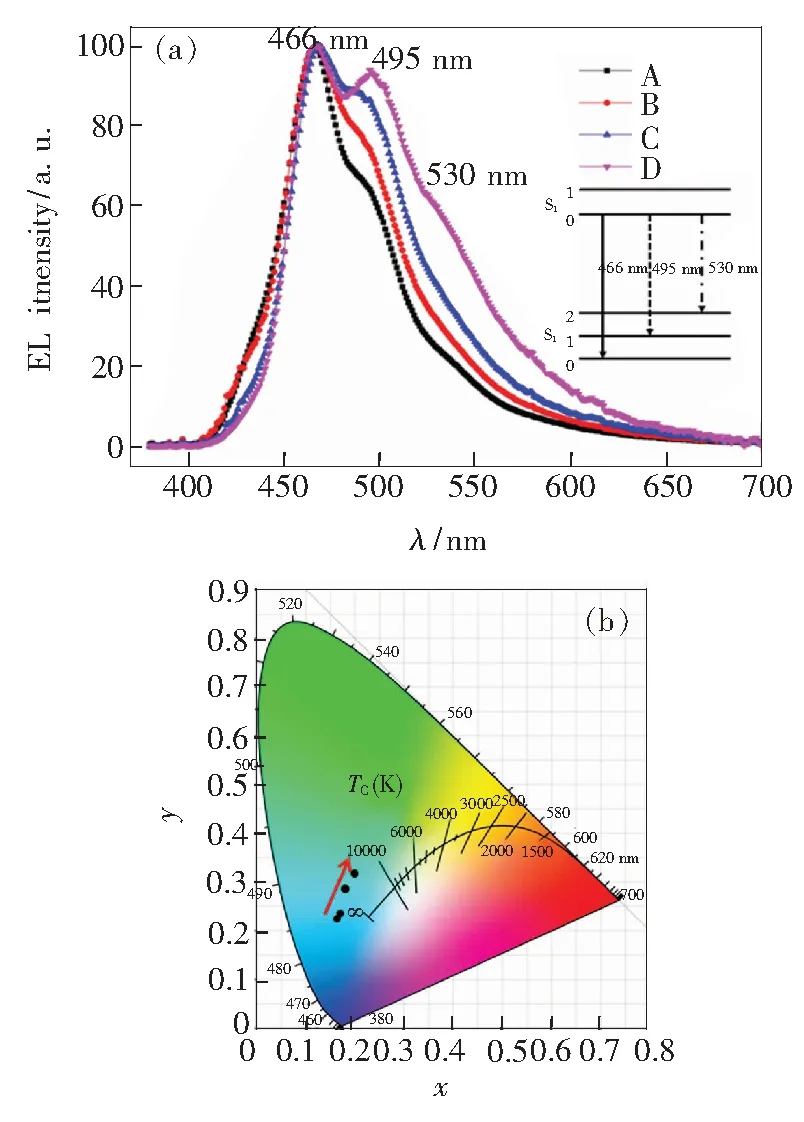
Fig.2 EL spectra (a) and CIE chromaticity coordinates (b) of device A
It is especially noted that a very weak emission is still observed at~430 nm, and the emission intensity at 430 nm increases with the decreasing of EML thickness, as shown in Fig.2(a). This can be ascribed to the emission of the MADN host, because it has an EL peak at 439 nm. However, it is more reasonable that the emission at 430 nm is attributed to formation of a second recombination region near the NPB/DPAVBI-doped MADN interface. This implies that the leakage of electrons from EML to HTL becomes more obvious with EML thickness decreasing, which is caused by the increasing electric field in the organic layer with EML thickness decreasing.
Fig.3(a) and (b) show the current density and luminancevs. the forward bias of device A with different EML thickness. It is observed the threshold voltage of the devices increases with the increasing of EML thickness, and a maximum luminance of 57 000 cd·m-2is obtained at 17 V when the blue EML thickness is 15 nm.
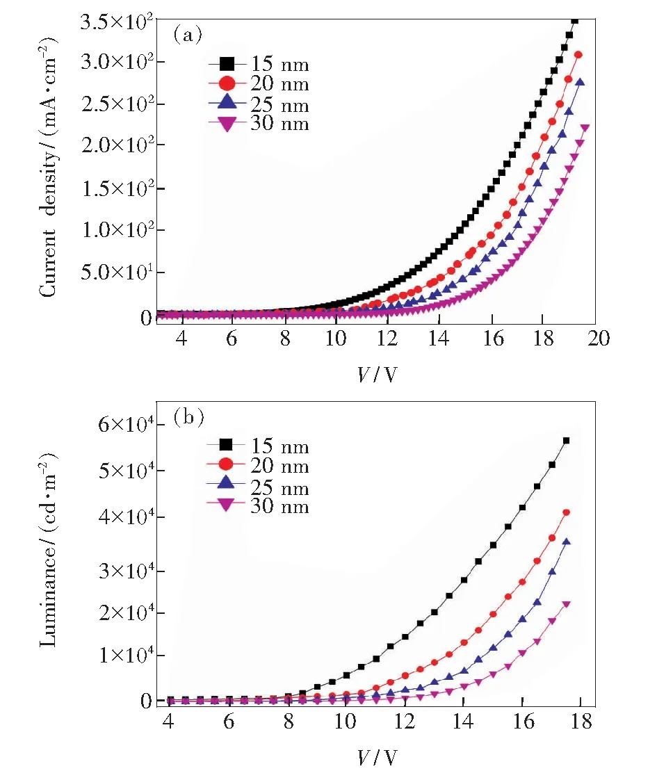
Fig.3 Current density-voltage (J-V) (a) and luminance-voltage (L-V) (b) curves of device A
The current efficiency is plottedvs. the current density for device A with different EML thickness, as shown in Fig.4(b). We observe that the current efficiency decreases with increasing EML thickness, and the current efficiency of all the devices slowly decreases with increasing current density. When the EML thickness varies from 15 to 30 nm, the corresponding highest current efficiency decreases from 47 to 30 cd·A-1. The maximum external quantum efficiency of the BOLEDs with the EML thinness of 15, 20, 25, 30 nm is 9.2%, 8.2%, 7.3% and 6.9%, respectively.
The EL spectra of WOLEDs are shown in Fig.5(a). The only difference between device B and C is the stack order of two emitting layers, as shown in Fig.1. The WOLED with an EML sequence of orange/blue is denoted device B and the other with an EML sequence of blue/orange is denoted device C. The EL spectra were obtained under the current density of 10 mA·cm-2and 150 mA·cm-2, respectively.
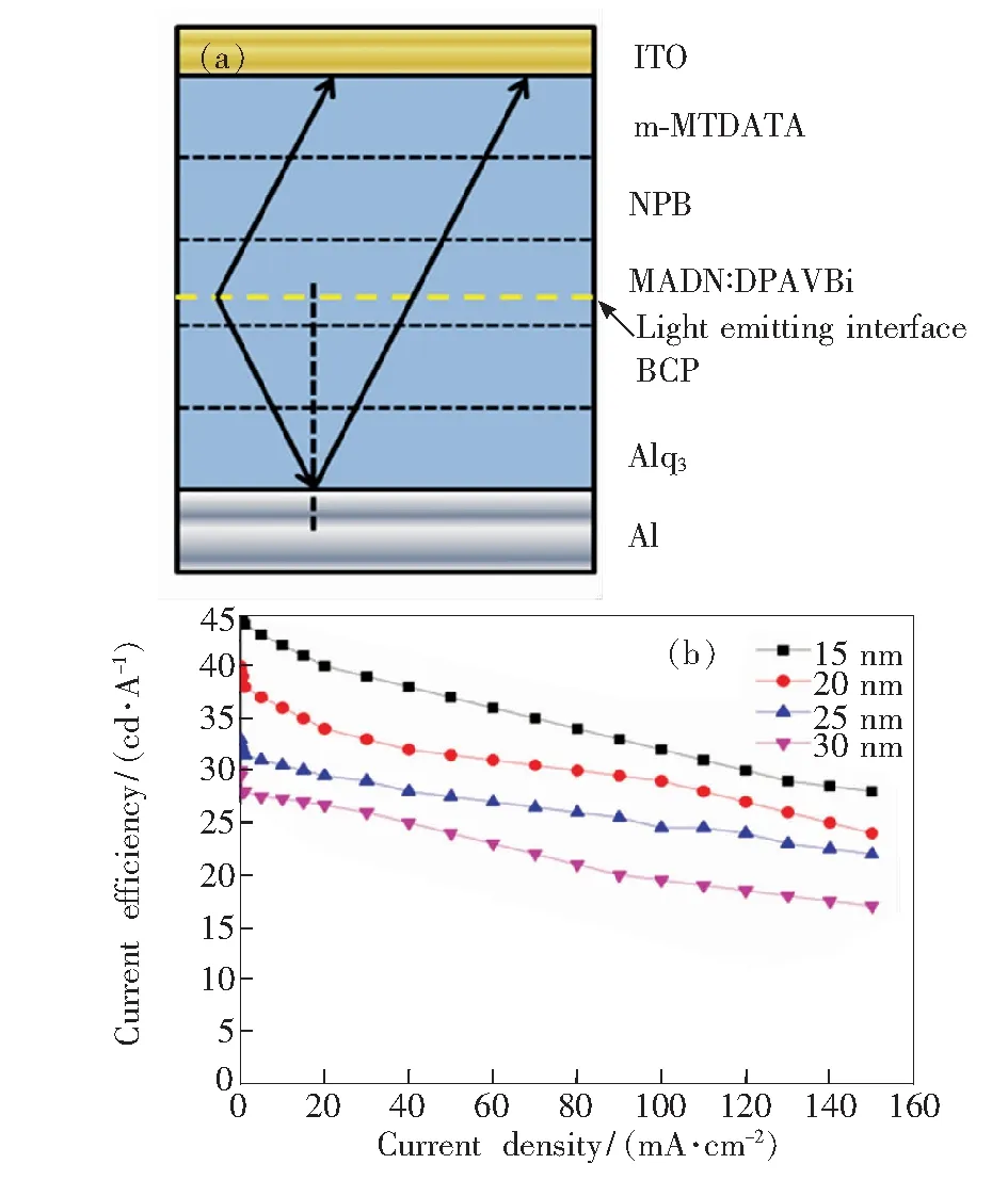
Fig.4 (a) Microcavity schematic of BOLED. (b) Current efficiency-current density characteristics of device A.
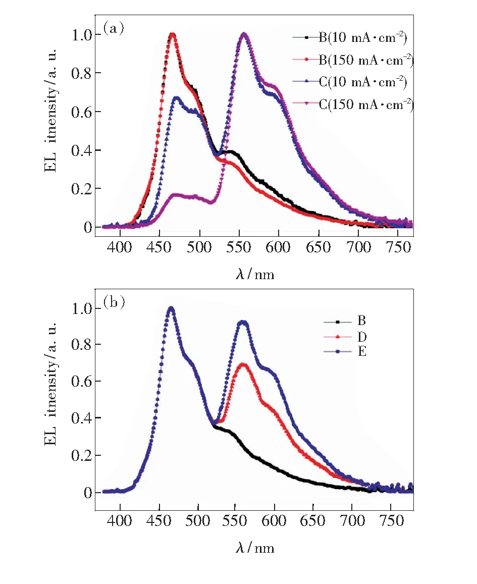
Fig.5 (a) EL spectra of device B and C at the current density of 10 mA/cm2and 150 mA/cm2, respectively. (b) EL spectra of B, D, E with the orange EML thickness of 5, 10, 15 nm, respectively.
From Fig.5(a), we can see that in device B the peak intensity of the blue emission is stronger than that of the orange emission, while the situation of device C is the reverse. This is due to the easier hole injection into organic layer than the electron injection. It can be seen from Fig.6 that the highest occupied molecular orbital (HOMO) level of m-MTDATA is 5.1 eV, which is 0.4 eV higher than the work function of ITO (4.7 eV). On the other hand, the work function of Al is 4.2 eV, which is 1.2 eV higher than lowest unoccupied molecular orbital (LUMO) level of Alq3. Thus, a very small hole injection barrier forms between ITO and m-MTDATA and leads to a strong hole injection from ITO to m-MTDATA comparing with the electron injection from Al to Alq3. As a result, most of the mobile carriers would recombine near the cathode. Nevertheless, an impressive phenomenon occurs that the peak intensity of orange emission weakens when the current density varies from 10 to 150 mA·cm-2in device B, while in device C the peak intensity of blue emission weakens under the same conditions. When the current density reaches 150 mA·cm-2, the peak intensity of orange emission in device B weakens slightly but the peak intensity of blue emission in device C weakens dramatically. The CIE coordinates of device B changes from (0.219 6, 0.292 5) to (0.204 7, 0.273 1), and that of device C variesaThe CIE of devices were measured at the current density 150 mA·cm-2from (0.364 3, 0.43 2) to (0.444 2, 0.483 3) when the current density varies from 10 to 150 mA·cm-2, as shown in Fig.7(a). The results show that device B behaves more steadily than device C at the same conditions. This may be attributed to the fact that Rb in the orange EML acts as a hole-trap sites[24-25], which can capture passing holes and reduce the hole mobility even at high current density and finally balance the concentration of electrons and holes between two EMLs.
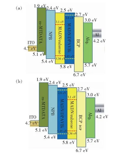
Fig.6 Energy band gap schematics of device B (a) and device C (b)
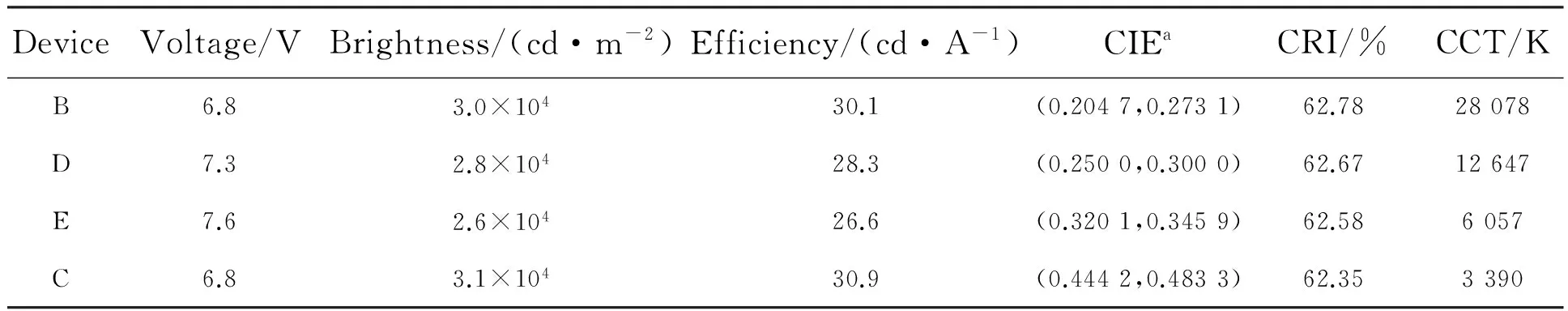
Table 2 Performance parameters of device B, C, D and E
The performance parameters of device B and C are listed in Table 2. Table 2 shows that the turn-on voltages of device B and C are basically same (both are 6.8 V), but the brightness of 31 600 cd/m2and the efficiency of 30.9 cd/A of device C are slightly greater than those of device B (30 800 cd/m2and 30.1 cd/A). This can be ascribed to a direct charge trapping mechanism. Rb has a lower LUMO and a higher HOMO compared with DPAVBi (see Fig.6). Therefore, the injected carriers can be more easily trapped by Rb[26]than by DPAVBi, and then a direct carrier recombination occurs at luminescent centers of Rb[27]. The color rendering index (CRI) and color temperature (CCT) are shown in Table 2.
Although the brightness and efficiency of device C are greater than device B, but the color stability of the latter is better than the former. In order to obtain a more desirable white device, we optimized the thickness of orange EML of device B and fabricated device D and E with the thickness of 10 and 15 nm, respectively. It is observed that the threshold voltage and the orange emission intensity of device B, D and E increase and the CIE coordinates of the devices get closer to standard white light with increasing orange EML thickness (see Fig.5(b) and 7(a)), and an optimal CIE coordinates of (0.320 1, 0.345 9) is obtained when the orange EML thickness is 15 nm,i.e., device E. And we see that the brightness and the efficiency of the devices decrease with orange EML thickness increasing.
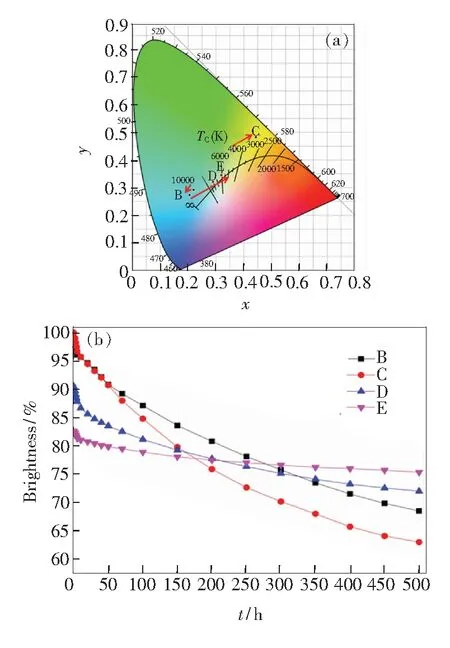
Fig.7 (a) CIE coordinates of device B, C, D and E, respectively. (b) Luminance of device B, C, D and E varies with time, respectively.
Fig.7(b) shows the luminance of device B, C, D and E with time. The brightness of all white light devices is normalized to the maximum brightness of device C. It is found that the brightness of all the devices decreases with time, the brightness of device B, C, D and E decays by 37.1%, 30%, 21%, 9% after 500 h, respectively. And we find that the decay rate of device B is slower than that of device C, this may be due to Rb in the orange EML that may act as hole trap sites. From Fig.6, we can see that the hole injection efficiency is higher than the electron, thus it is reasonable that the holes would be more than the electrons in device B and C. But Rb in the orange EML in device B can act as hole trap sites and capture passing holes, this balances the concentration of electrons and holes and therefore prolongs the device lifetime[28]comparing with device C. After thickness optimization of device B, the decay rate of the optimized devices (device D and E) becomes slower further.
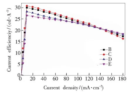
Fig.8 Efficiency-current density characteristics of WOLEDs
The efficiency plots of white OLEDs are shown in Fig.8. Form Fig.8, we can see that the maximum efficiency of device B, C, D, E is 30.1, 30.9, 28.3, 26.6 cd/A, respectively. The maximum efficiency of device C is larger than that of any other device, but the decay rate of device C is faster than that of any other one, this may be due to Rb in the orange EML that can act as hole trap sites.
4 Conclusion
In this study, BOLEDs with an EML of MADN∶DPAVBi were successfully fabricated. It is observed that the EL spectra, current efficiencies, operational voltage and operational current density strongly depend on the EML thickness of BOLEDs. By adjusting the thickness of the blue EML, the EL spectra of the BOLEDs can be tuned from blue to green-blue. A maximum luminance of 57 000 cd·m-2and current efficiency of 47 cd·A-1(under illumination of 1 000 cd·m-2) are obtained when the thickness of the BOLED is 15 nm. After that, WOLEDs with blue and orange EMLs were fabricated. The efficiency, lifetime, brightness, spectral voltage-dependence and white balance of the WOLEDs were studied. The results demonstrate that the performance of the WOLEDs is strongly linked to the stack order of two EMLs and the thickness of the EML, which may be due to Rb in orange EML in device B (WOLED with an EML sequence of orange/blue) that can capture the passing holes and hence balance the concentration of electrons and holes. Subsequently, we optimized the orange EML thickness of device B and a favorable CIE coordinates of (0.320 1, 0.345 9) is achieved when the orange EML thickness is 15 nm (i.e., device E).
[1] Chang K D, Li C Y, Pan J W,etal. A hybrid simulated method for analyzing the optical efficiency of a head-mounted display with a quasi-crystal OLED panel [J].Opt.Express, 2014, 22(s2):A567-A576.
[2] Liao Y Q, Gan Z H, Liu X Y. Improvement of OLED performance by using DPVBi as hole-blooking layer [J].Chin.J.Lumin.(發光學報), 2011, 32(10):1041-1045 (in Chinese).
[3] Cheng C R, Chen Y H, Qin D S,etal. Lithium carbonate doped 3, 4, 9, 10-perylenetetracarboxylic dianhydride for enhanced performance in organic light emitting diode [J].Chin.J.Lumin.(發光學報), 2011, 32(4):387-392 (in Chinese).
[4] Cho A R, Kim E H, Park S Y,etal. Flexible OLED encapsulated with gas barrier film and adhesive gasket [J].Synth.Met., 2014, 193:77-80.
[5] Burroughes J H, Bradley D D C, Brown A R,etal. Light-emitting diodes based on conjugated polymers [J].Nature, 1990, 347(6293):539-541.
[6] Mauser N, Hartmann N, Hofmann M S,etal. Antenna-enhanced optoelectronic probing of carbon nanotubes [J].NanoLett., 2014, 14(7):3773-3778.
[7] Tseng S R, Meng H F, Lee K C,etal. Multilayer polymer light-emitting diodes by blade coating method [J].Appl.Phys.Lett., 2008, 93(15):153308-1-3.
[8] Dong M, Zhong L. Chameleon: A color-adaptive web browser for mobile OLED displays [J].IEEETrans.MobileComput, 2012, 11(5):724-738.
[9] Kessler F, Watanabe Y, Sasabe H,etal. High-performance pure blue phosphorescent OLED using a novel bis-heteroleptic iridium (Ⅲ) complex with fluorinated bipyridyl ligands [J].J.Mater.Chem.C, 2013, 1(6):1070-1075.
[10] Shi J, Tang C W. Anthracene derivatives for stable blue-emitting organic electroluminescence devices [J].Appl.Phys.Lett., 2002, 80(17):3201-3203.
[11] Swanson S A, Wallraff G M, Chen J P,etal. Stable and efficient fluorescent red and green dyes for external and internal conversion of blue OLED emission [J].Chem.Mater., 2003, 15(12):2305-2312.
[12] Su S J, Gonmori E, Sasabe H,etal. Highly efficient organic blue-and white-light-emitting devices having a carrier-and exciton-confining structure for reduced efficiency roll-off [J].Adv.Mater., 2008, 20(21):4189-4194.
[13] Yongá C H. Highly rigid and twisted anthracene derivatives: A strategy for deep blue OLED materials with theoretical limit efficiency [J].J.Math.Chem., 2012, 22(6):2695-2700.
[14] Yeh S J, Wu M F, Chen C T,etal. New dopant and host materials for blue-light-emitting phosphorescent organic electroluminescent devices [J].Adv.Mater., 2005, 17(3):285-289.
[15] Ummartyotin S, Juntaro J, Sain M,etal. Development of transparent bacterial cellulose nanocomposite film as substrate for flexible organic light emitting diode (OLED) display [J].IndustrialCropsandProducts, 2012, 35(1):92-97.
[16] Reineke S, Lindner F, Schwartz G,etal. White organic light-emitting diodes with fluorescent tube efficiency [J].Nature, 2009, 459(7244):234-238.
[17] Geffroy B, Le Roy P, Prat C. Organic light-emitting diode (OLED) technology: Materials, devices and display technologies [J].Polym.Int., 2006, 55(6):572-582.
[18] Ren X, Li J, Holmes R J,etal. Ultrahigh energy gap hosts in deep blue organic electrophosphorescent devices [J].Chem.Mater., 2004, 16(23):4743-4747.
[19] Wang D, Wu Z, Lei X,etal. Electroluminescence of solution-processed organic light-emitting diodes based on fluorescent small molecules and polymer as hole-transporting layer [J].Phys.Stat.Sol.(a), 2013, 210(12):2556-2560.
[20] Li C, Tsuboi T, Huang W. Characteristics of blue organic light emitting diodes with different thick emitting layers [J].Opt.Mater., 2014, 36(10):1720-1723.
[21] Hsiao C H, Lin C F, Lee J H. Driving voltage reduction in white organic light-emitting devices from selectively doping in ambipolar blue-emitting layer [J].J.Appl.Phys., 2007, 102(9):094508-1-6.
[22] Wu Z, Wang L, Lei G,etal. Investigation of the spectra of phosphorescent organic light-emitting devices in relation to emission zone [J].J.Appl.Phys., 2005, 97(10):103105-1-6.
[23] Riel H, Karg S, Beierlein T,etal. Phosphorescent top-emitting organic light-emitting devices with improved light outcoupling [J].Appl.Phys.Lett., 2003, 82(3):466-468.

[25] Chin B D, Kim J K, Park O O. Controlled light emission from white organic light-emitting devices with a single blue-emitting host and multiple fluorescent dopants [J].J.Phys. D:Appl.Phys., 2007, 40(15):4436-4441.
[26] Zheng X Y, Zhu W Q, Wu Y Z,etal. A white OLED based on DPVBi blue light emitting host and DCJTB red dopant [J].Displays, 2003, 24(3):121-124.
[27] Zhao J, Yu J, Liu S,etal. Combined host-guest doping and host-free systems for high-efficiency white organic light-emitting devices [J].J.Lumin., 2012, 132(8):1994-1998.
[28] Meerheim R, Scholz S, Olthof S,etal. Influence of charge balance and exciton distribution on efficiency and lifetime of phosphorescent organic light-emitting devices [J].J.Appl.Phys., 2008, 104(14):014510-1-8.
1000-7032(2015)07-0821-08
Influence of Light-emitting Layer Position on White Organic Light-emitting Diodes
XIANG Dong-xu1, LI Hai-rong1,2,3*, XIE Long-zhen1, YANG Jia-ming1, WANG Fang1, YUAN Chao-xin1, SUN Yong-zhe1
(1.InstituteofMicroelectronics,SchoolofPhysicalScienceandTechnology,LanzhouUniversity,Lanzhou730000,China; 2.KeyLaboratoryforMagnetismandMagneticMaterialsofTheMinistryofEducation,LanzhouUniversity,Lanzhou730000,China; 3.KeyLaboratoryofSpecialFunctionMaterialsandStructureDesign,MinistryofEducation,Shanghai200050,China)*CorrespondingAuthor,E-mail:hrli@lzu.edu.cn
Two types of white organic light-emitting devices (WOLED) containing a layered light-emitting region composed of a single blue-emitting host and different fluorescent dopants (blue and orange) were fabricated. The efficiency, lifetime, brightness, spectral voltage-dependence and white balance of devices were investigated. The results show that the performance of the devices strongly depends on the stack order of two emitting layers and the thickness of the emitting layer. It is found that the WOLED with an EML sequence of orange/blue (from anode to cathode) shows better stability than that with an EML sequence of blue/orange. It is due to the rubrene in orange emitting layer that acts as hole-trap sites and captures the passing holes and hence balances the concentration of electrons and holes. The optimized white device exhibits a favorable CIE coordinates (0.320 1, 0.345 9) which is close to the standard white light.
organic electroluminescent; light-emitting layer sequence and thickness; carrier injection; carrier balance
TN383+.1 Document code: A

向東旭(1988-),男,湖北隨州人,碩士研究生,主要從事有機半導體器件的研究。Email: xiangdx12@lzu.edu.cn

李海蓉(1971-),女,甘肅臨洮人,教授,2004年于蘭州大學獲得博士學位,主要從事半導體光電子學方面的研究。Email: hrli@lzu.edu.cn
10.3788/fgxb20153607.0821
2015-04-13;
2015-05-05
甘肅省自然科學基金(1107RJZA090); 蘭州大學磁學與磁性材料教育部重點實驗室開放課題; 信息功能材料國家重點實驗室開放課題(12-668)資助項目
猜你喜歡
電子競技(2020年8期)2020-12-23 04:09:40
電子競技(2020年7期)2020-10-12 10:45:48
電子競技(2020年5期)2020-08-10 08:43:10
電子競技(2020年4期)2020-07-13 09:18:06
電子競技(2020年2期)2020-04-14 04:40:38
電子競技(2020年11期)2020-02-07 02:49:36
電子競技(2020年9期)2020-01-11 01:06:21
電子競技(2020年10期)2020-01-11 01:06:06
電子競技(2019年22期)2019-03-07 05:17:26
電子競技(2019年21期)2019-02-24 06:55:52