Design of Thermopile-Based Infrared Detectors with Suspended Absorber-Thermopile Bi-Layers*
2014-12-06 08:30:22CHENYuanjingMAOHaiyangTANQiulinXUEChenyangOUWenCHENDapengXIONGJijun
傳感技術學報 2014年6期
CHEN Yuanjing,MAO Haiyang,3* ,TAN Qiulin,XUE Chenyang,OU Wen,CHEN Dapeng,XIONG Jijun
(1.Key Lab of Instrumentation Science and Dynamic Measurement,North University of China,Taiyuan 030051,China;2.Key Laboratory of Microelectronics Devices and Integrated Technology,Institute of Microelectronics,Chinese Academy of Sciences,Beijing 100029,China;3.Smart Sensor Engineering Center,Jiangsu R&D Center for Internet of Things,Wuxi 214135,China)
IR detectors have been widely used in both military and civilian fields,the applications include night-vision equipment,missile guidance,military security[1-3],thermograph[1],gas analysis[4],and others.Thermopile IR devices based on Seebeck principle are one type of the most important IR detectors,as they need neither cooling system,nor chopper,and moreover,they are compatible with both dynamic and static test systems.
IR detectors with coplanar absorber-thermopile single-layers have been reported[5-8]with releasing windows opened on the absorber layer,which results in loss of absorption and hinder of heat conduction.For those coplanar designs,the absorbing areas and the thermopiles are usually distributed side-by-side in a relatively large scale,thus the dimensions of the devices are difficult to be scaled down.
To ensure structural integrity of the absorber and to improve space utilization[9],non-coplanar IR structures have been studied.The most representative example is Toriyama’s vertical thermopiles bending with tensile stress,in this device,however,the structure for supporting absorber is not stable[7].In order to reduce the release difficulties and improve thermal conduction,Marc C.Foote presented a tri-layer structure based on polyimide sacrificial bi-layers.In this structure,Bi-Te and Bi-Sb-Te are used as the thermopile materials,and meanwhile,thermal contact is located at the center of the sensor[10].However,the compatibility of the thermopile materials with Micro-Electro-Mechanical Systems(MEMS)fabrication remains an unsolved problem.In additional,hot posts of thermopiles are distributed on both sides of the absorber,which may cause unavoidable thermal crosstalk.
A thermopile-based IR detector is designed and presented in this work.In this detector,polyimide sacrificial layer with inclined sidewalls is formed for thermal contact between the absorber and the thermopiles,and also used to support the absorber.The cold posts of the thermopiles are set in the middle of the sensing area to realize better cooling ability,less thermal stress and low thermal interference.Moreover,this bi-layer structure achieves high thermoelectric conversion in a relatively small area.Subsequently,according to the one-dimensional thermal conduction theory,a simplified model is established and used to simulate the performances of the detectors.Furthermore,fabrication process of the detectors is also investigated.
1 Methodology
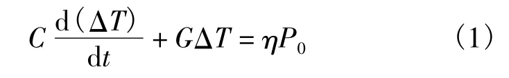
The thermal equilibrium in IR detectors follows the energy conservation principle concerning the absorbed heat,the conductive heat and the radiant heat.When thermal conversion and radiation process are got ignored in the vacuum packaging conditions,a thermal conduction system can be simplified into a one-dimensional model,as shown in Eq.1.
Herein,C and G represent heat capacity and heat conductivity,respectively,η is the IR absorptance of the absorber.In this equation,stands for the thermal power in conductive way,GΔT refers to power
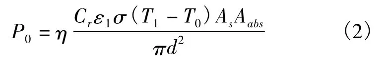
Where Cris the root mean square conversion factor,Asis the area of the whole sensor,d is the distance between blackbody and the absorber.T0and T1stand for temperature of environment and the blackbody furnace,respectively.Consequently,the temperature difference ΔT is obtained as in capacitive way,while ηP0is the derived heat.The absorber with an area of Aabsis taken as part of a sphere in space radiation,thus the IR radiation absorbed by the absorbing area can be approximated as
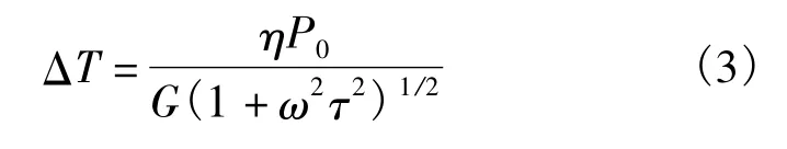
In this equation,τ is the response time of the device.When ωτ→0,Eq.3 could be simplified to Eq.4,which demonstrates that the temperature difference is determined by the derived heat and the conduction.
Subsequently,the responsivity Rvand detectivity D*are calculated as
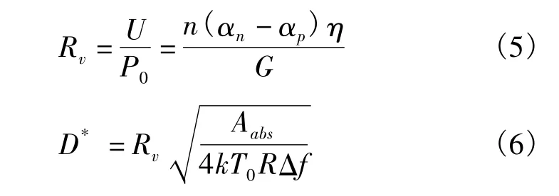
Herein,R represents the total resistance of the detector,and Δf can be obtained from Δf=f/Q.The energy transformation from IR incidents to voltage output can be divided into two related steps,which are opticalthermal conversion realized in the IR absorber,and thermal-electrical conversion realized through the thermopiles.The conductivity and capacity of the device can be approximated toand C= ρcV,respectively.Meanwhile,the response time τ,and noise equivalent power NEP are also obtained
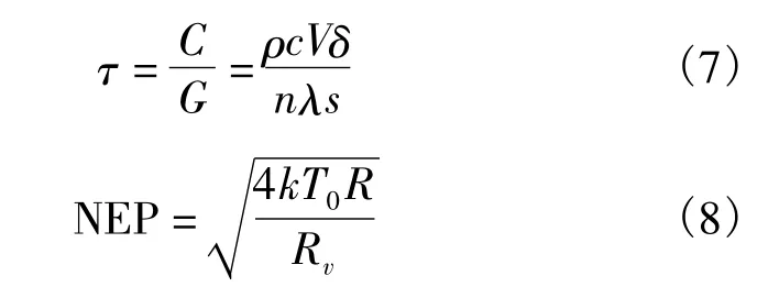
In Eq.7,s refers to cross-section area of a thermo-electrode in the thermocouple,c is the specific heat of the absorber,G represents conductivity of the device,and δ is the effective conductive length.
2 Structural Design
2.1 Design of the non-coplanar models
Design of the IR detectors aims at achieve a perfect structural stability,high-yield,superior properties and so on.The following methods are required to achieve the above principles.First of all,layers except for the thermopiles should be thinning to decrease thermal capacity in the IR device,which will otherwise prolong the response time and increase residual thermal stress.Secondly,the three-dimensional vision,like bi-layer ideal,works for reducing fabrication cost and scaling down the size.At last,with IR design researches deeply,cooling system and thermal isolation technology has been introduced to structure design fields to lower thermal interference during characteristic improving process.Above all,one of the most effective way to evaluate the structure of IR detectors is thermocouple temperature difference during testing process.
Simulations of thermal distribution are carried out using a single-layer IR detector and a bi-layer IR detector as the models,where both structures are limited to an area of 300 μm ×300 μm.The length of the thermocouple is set as 150 μmm with their cold-sinking structures at the device center.In such a model,the initial temperature of the substrate is 313.15℃.When the absorber gains heat power of 1 nW/μm2,the temperature difference between the hot post and cold post in the single-layer IR model reaches 0.1 ℃,the results are shown in Fig.1.
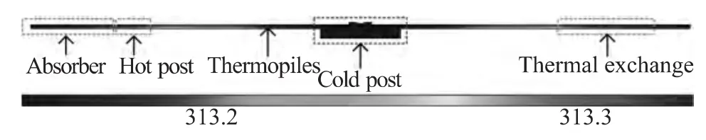
Fig.1 Thermal simulation of a single-layer IR detector model
The performances of the single-layer detector are faced with difficulty due to the contradiction between the increasement of the absorbing area and the thermocouple length at the same time.On the other hand,the absorbing area in the bi-layer detector can reach as large as 300 μm ×300 μm,which is also the whole area of the device.The thermal simulation results demonstrate that with the same radiation conditions,the temperature difference in the bi-layer model increases to 0.85 ℃,shown in Fig.2.
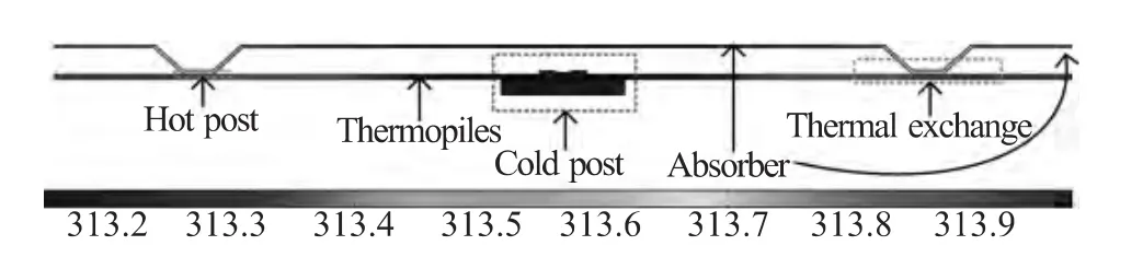
Fig.2 Thermal simulation of a bi-layer IR detector model
According to the simulation results,the temperature difference of the bi-layer mode is 0.75 ℃ higher than that of the single-layer structure.The enhanced temperature difference will further contribute to an increased voltage response.Therefore,in our design,the bi-layer structure is employed in the IR detectors with only its cold posts contacting with the substrates.
2.2 Design of the IR device
In order to reduce the thermal loss in a structure with high stability,absorber-thermopile bi-layers are utilized in the device.Herein,an inverse trapeziums structure is adopted as the supporter and the thermal conductor between the two layers.Such a novel design provides an approach to reduce the thermal loss by releasing both sacrificial layers thus to suspend the bilayers,as shown in Fig.3.In the structure,the absorber and the thermopiles are isolated from each other by the cavities,and the heat is transferred from the absorber to the hot posts of the thermopiles.Subsequently,the heat is transferred from the hot posts to the cold posts as the Si substrate functions continually as a cooler for the cold posts.Ascribed to the reduction of the heat capacity,temperature difference between the two posts is enhanced,which may largely improve the performance and achieve a smaller size of the device.
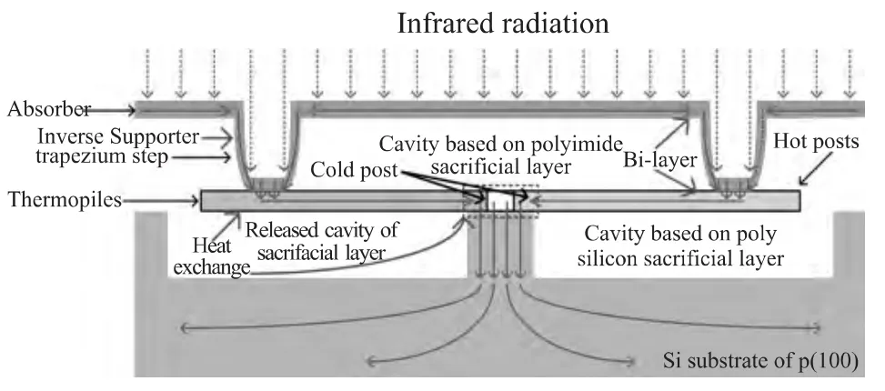
Fig.3 Structure of the thermopile-based IR device and the thermal conduction within the structure
Table 1 demonstrates relations between some parameters and characteristics of the device.Taking the parameters,including length,width and thickness of the thermopiles as individual variables at each time,the effects of their variations on the RV,D*,τ,NEP,and NETD are studied.It should be noted that the maximum D*can be achieved when thermopile width is 2 μm.Then thickness can be set as 0.3 μm via balancing the relationship between RVand D*.Consequently,a length of 125 μm is determined to realize a small τ.In the device,the thermopiles are connected into series of 50 couples for larger voltage output.Taking the optimized parameters as shown in Table 2 into consideration in the one-dimension thermal conduction model,the D*,RVand τ of the IR detector are calculated to be 2.85 ×10⁸cmHz(1/2)/W,1 800 V/W and 6 ms,respectively.In such a device,complex absorber based on SiO2-Si3N4-SiO2is adopted.In Table 3,comparisons of performances are made between the reported IR devices and ours.
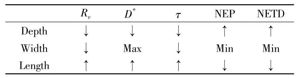
Table 1 Effects of structural parameters on device characteristics
*↓stands for negative correlation between parameter and characteristic;↑stands for positive correlation between parameter and characteristic;Max means the characteristic achieves its maximum value during parameter variation;Min means the characteristic achieves its minimum value during parameter variation.
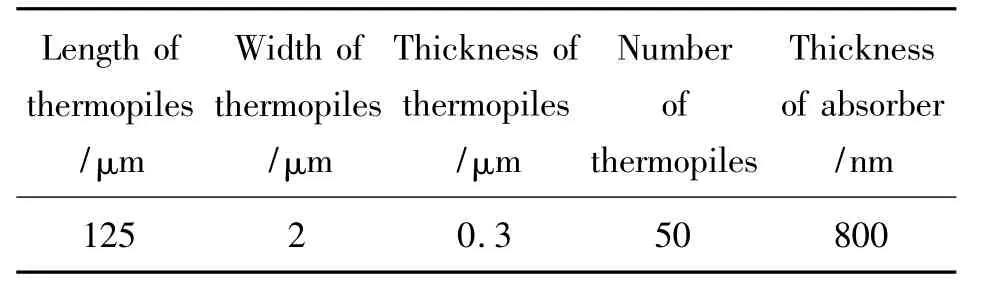
Table 2 Optimized values of the structural parameters
In table 3,the bi-layer IR detector with optimized size is comparing with a few advanced researches.With a smaller cell size as 300 μm × 300 μm,the response characteristic of the bi-layer IR detector is almost 18 times higher than others.In additional,the detectivity of the bi-layer IR detector achieves to be more than twice higher than other IR detectors.Furthermore,the bi-layer IR detector reaches lower response time.
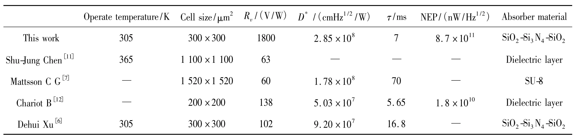
Table 3 Performance comparison with IR detectors reported in references
3 Fabrication
3.1 Fabrication of non-coplanar models
The bi-layer structures can be realized by using two sacrificial layers including polyimide and a siliconbased film.In detail,the depositions of the Poly-Si based thermopile layers require high temperature,therefore,polyimide is not a suitable sacrificial material beneath the thermopiles.In order to suspend the thermopiles,the silicon substrate is partially etched.That is to say,separated sacrificial layers,composed of polyimide and the silicon substrate are employed respectively to realize the absorber-thermopile bi-layers.
Figure.4 describes the process for fabricating the non-coplanar sacrificial layer of polyimide.Firstly,polyimide is spin-coated on an oxide layer,and then covered by another silicon oxide deposited by PECVD(plasma enhanced chemical vapor deposition).Later on,the polyimide coating is photo-patterned by using the top-layer dioxide as the hard-mask material in an etching circumstance,where the etching gases are mixed at a rate of SF6∶O2=30 sccm∶40 sccm.In this way,a perfect inverse trapezium structure can be achieved.After removal of the hard-mask layer with BOE(buffered oxide etching solutions),IR absorbing material can be deposited with very low roughness and low thermal stress.
3.2 Fabrication of the device
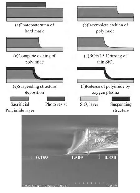
Fig.4 Fabrication process for a non-coplanar structure and image of an inverse trapezium structure of polyimide
The fabrication process of the IR device is schematically illustrated in Fig.5.At the beginning of the process,a SOI substrate is prepared,and narrow trenches are etched on the top silicon layer and then the trenches are filled with TEOS(Fig.5(a)).Later on,a Poly-Si layer alternatively implanted with B+and P-ions are photo-patterned into P-type and N-type thermopiles(Fig.5(b)).After metal sputtering and electrode-patterning,another layer of dioxide with a thickness of 1 000 ? is deposited on the top as a passivation layer.Subsequently,releasing windows are opened before polyimide(3 μm in thickness)is coated(Fig.5(c)~5(e)).After spin-coating of the polyimide layer,two inverse trapezium structures are generated,which will further be used as the supporter for the absorber.To protect the low-stress SiNxlayer,thin SiO2films are also deposited to form a SiO2-Si3N4-SiO2structure,shown in Fig.5(f).In the release process,the no-coplanar structure is firstly formed by removal of the polyimide sacrificial layer using oxygen plasma(Fig.5(g)).Subsequently,the entire device is released by etching the top silicon layer of the original SOI substrate.In the XeF2-based front etching process,the trenches filled with TEOS are utilized as etching stops(Fig.5(h)).
4 Conclusion
Fig.5 Fabrication process of the thermopile-based IR detector
In this work,a thermopile-based IR detector with high performances and a small size is designed.In this detector,suspended absorber-thermopile bi-layers are utilized to enhance thermocouple temperature difference with perfect structural stability and high-yield conversion,meanwhile cold posts are distributed at the center of the device for faster cooling way.The detectivity,responsibility and response time of the IR detector are calculated to be 2.85 ×10⁸cmHz(1/2)W(-1),1 800 V/W and 6 ms,respectively.In addition,a CMOS-compatible fabrication process is also presented.This IR detector is expected to find applications in gas analysis,environment monitoring,blackbody furnace,and so on.
Kowledgement
This work is supported in part by the National Natural Science Foundation of China(Grant No.61335008 and 51205373),Jiangsu Natural Science Foundation(Grant No.BK20131098),and Shanxi Province NaturalScience Foundation(GrantNo.2012021013-4).
[1]Houlet L F,Shin W,Tajima K,et al.Thermopile Sensor-Devices for the Catalytic Detection of Hydrogen Gas[J].Sensors and Actuators B:Chemical,2008,130(1):200-206
[2]Charlton D E.Recent Developments in Cadmium Mercury Telluride Infrared Detectors[J].Journal of Crystal Growth,1982,59(1):98-110.
[3]Golubovic D S.Analysis of Heterojunction Resonant Cavity-Enhanced Schottky Photodiodes by Using Two-Valley Transport Model[J].Infrared Physics and Technology,2002,43(6):327-334.
[4]Van Herwaarden A W,Van Duyn D C,Van Oudheusden B W,et al.Integrated Thermopile Sensors[J].Sensors and Actuators A:Physical,1989,22(1):621-630.
[5]Mattsson C G,Bertilsson K,Thungstr?m G,et al.Thermal Simulation and Design Optimization of a Thermopile Infrared Detector with an SU-8 Membrane[J].Journal of Micromechanics and Microengineering,2009,19(5):055016.
[6]Xu D,Xiong B,Wang Y.Design,Fabrication and Characterization of a Front-Etched Micromachined Thermopile for IR Detection[J].Journal of Micromechanics and Microengineering,2010,20(11):115004.
[7]Toriyama T,Yajima M,Sugiyama S.Thermoelectric Micro Power Generator Utilizing Self-StandingPolysilicon-MetalThermopile[C]//Micro Electro Mechanical Systems,2001.MEMS 2001.The 14th IEEE International Conference on IEEE,2001:562-565.
[8]Xia Y,Xue C,Qu W,et al.A Design of Thermopile Infrared Detector Based on Black Silicon As Absorption[J].Chinese Journal of Sensors and Actuators,2012(5):007.
[9]Zhao L J,Ou W,Yan J H,et al.Fabrication of a Thermopile Infrared Detector That Compatible with CMOS Process[J].Infrared Technology,2012(2):007.
[10]Foote M C,Gaalema S D.Progress Toward High-Performance Thermopile Imaging Arrays[C]//Aerospace/Defense Sensing,Simulation,and Controls.International Society for Optics and Photonics,2001:350-354.
[11]Chen S J,Shen C H.A New Investigation of High-Frequency Thermopile Response[C]//Microelectronics,MEMS,and Nanotechnology.International Society for Optics and Photonics,2005:603518-603518-8.
[12]Charlot B,Parrain F,Mir S,et al.Self-Testable CMOS Thermopile-Based Infrared Imager[C]//Design,Test,Integration,and Packaging of MEMS/MOEMS 2001.International Society for Optics and Photonics,2001:96-103.